Optical grid for high precision and high resolution method of wafer-scale nanofabrication

a nanofabrication and optical grid technology, applied in the field of nanofabrication and nanometrology methods and to high resolution systems, can solve the problems of increasing the time needed for high resolution wafer fabrication, requiring considerable mass of the moving stage, and requiring high precision and precision control structural elements and sensors. achieve the effect of high precision and high resolution wafer-scale nano-metrology

Active Publication Date: 2011-10-13
CORNELL UNIVERSITY
View PDF1 Cites 12 Cited by
  • Summary
  • Abstract
  • Description
  • Claims
  • Application Information

AI Technical Summary

Benefits of technology

[0012]The present invention addresses the foregoing need through provision of an economical and reliable meth

Problems solved by technology

The precision and speed of the nanofabrication process is therefore dependent in part, on the precision of the stage's placement, and the movable stage is made of expensive and precisely controlled structural elements and sensors.
The stage must therefore have considerable mass, and the time taken to move that mass and then confirm or adjust the stage's position adds to the time needed for high resolution fabrication for any wafer having a large area.
Complex systems which integrate, for example, beam deflection control and stage movement control necessarily require considerable care in development and operation and those systems can be very expensive to configure and calibrate.
Broadly speaking, the problem is determining the position of an object in 3D space with nanometer precision, which is stable over long periods of time.
These motors have considerable hysteresis and motion characteristics change due to aging of components and interfaces between components, both introducing sources of error in position control.
The errors can be significant and if the probe is controlled to go back to a pre-defined starting position by following the motor's action in reverse, the probe can be off by distances too large compared to features that are of interest.
The aging and hysteresis errors affect the capability of the scanning probe to arrive at a given location and therefore when different samples are scanned, considerable time and effort is expended to find the location by scanning.
This can be detrimental to scanning for defects in nano-manufacturing, inc

Method used


Image

  • Optical grid for high precision and high resolution method of wafer-scale nanofabrication
  • Optical grid for high precision and high resolution method of wafer-scale nanofabrication
  • Optical grid for high precision and high resolution method of wafer-scale nanofabrication

Examples


Embodiment Construction

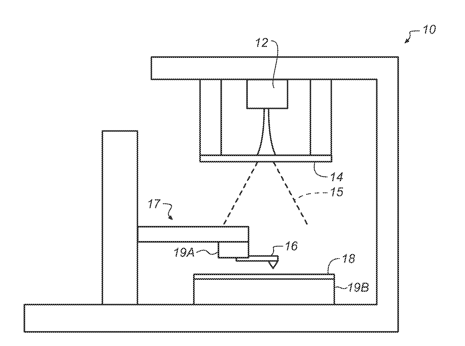
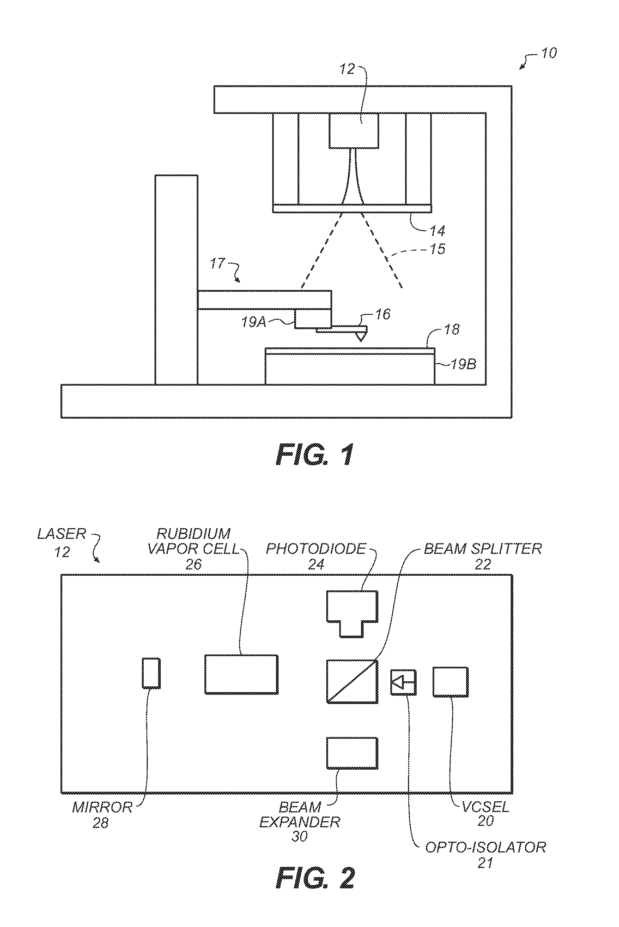
[0031]With reference to FIGS. 1-6B, an early prototype nano-optical ruler imaging system 10 includes a frequency stabilized laser 12 configured to aim a laser beam downwardly through an optical tether wafer (or “OTW”) 14 to project a high precision optical ruler 15 in space, which impinges upon a nano fabrication element (e.g., such as scanning probe 16 and a manufacturing wafer 18).

[0032]Scanning probe 16 is carried by any stable, movable, and controllable mechanism 17 that can movably position scanning probe 16 in any position needed to effectuate a fabrication process step anywhere on the upper or proximal surface of manufacturing wafer 18. In a preferred embodiment controllable mechanism 17, including a fine resolution X-Y-Z (3 axis) controller 19A and a coarse X-Y (2 axis) stage controller 19B are each configured to respond to control signals used to change the position of tool or nano fabrication element relative to the upper or proximal surface of manufacturing wafer 18.

[0033...


PUM


Abstract

A wafer-scale nano-metrology system (10) for sensing position of a nanofabrication element (16) when illuminated by a patterned optical projection defining a grid or position measuring gauge includes a frequency stabilized laser emitter (12) configured to generate a laser emission at a selected frequency, where the laser emission forms a diverging beam configured to illuminate a selected area occupied by a target fabrication object (18) having a proximal surface. An optical pattern generator (14) is illuminated by laser (12) and generates a patterned optical projection grid or gauge for projection upon the target fabrication object (18). A movable tool or nanofabrication element (16) carries an optical sensor array (50), and the sensor array detect at least a portion of the optical projection grid, and, in response to that detection, generates grid position data for use in controlling the position of the tool (16).

Description

CROSS REFERENCE TO RELATED APPLICATIONS[0001]This application is a national stage application under 35 U.S.C. §371 of PCT Application No. PCT / US2009 / 056400, filed Sep. 9, 2009, which claims the benefit of and priority to U.S. Provisional Patent Application No. 61 / 136,493 filed on Sep. 9, 2008, the entire disclosure of which is incorporated herein by reference.BACKGROUND OF THE INVENTION[0002]1. Field of the Invention[0003]The present invention relates in general to nanofabrication and nanometrology methods and to high resolution systems for manufacturing and measuring very small structures in wafers and substrates.[0004]2. Description of the Background Art[0005]High Resolution nanofabrication on a manufacturing wafer is required when manufacturing integrated circuits (ICs) including millions of microscopic circuit elements on the surface of tiny chips of silicon taken from the wafer, which is typically made of Silicon or Polysilicon, and other semiconductor materials. These chips ar...

Claims


Application Information

Patent Timeline
IPC IPC(8): G01B11/14B82Y40/00
CPCB82Y10/00B82Y35/00G01B11/25G03F7/7085G01Q40/02G01Q80/00G03F7/70383G01B11/2518
Inventor LAL, AMITYOSHIMIZU, NORIMASA
Owner CORNELL UNIVERSITY
Why Eureka
Try Eureka