
Method and apparatus for forming MEMS device

Active Publication Date: 2011-10-20
MASSACHUSETTS INST OF TECH
View PDF6 Cites 55 Cited by
  • Summary
  • Abstract
  • Description
  • Claims
  • Application Information

AI Technical Summary

Benefits of technology

[0012]In another embodiment, the disclosure relates to a MEMS sensor having a plurality of cavities (or holes) projecting from a substrate. The plurality of cavities can be arranged in an array with each cavity having a hollow interior separating a top portion and a bottom portion thereof. One or more diaphragm layers can be formed over the array. The first electrodes can communic

Problems solved by technology

However, the conventional methods are limited to working within the existing silicon semiconductor-based framework.
Several challenges, including expense, limited size and form-factor, and a restricted materials set, prevent the future realization of new MEMS for applications beyond single chip or single sensor circuits.
Standard processing techniques are particularly restrictive when considering expanding into large area fabrication.
Conventional photolithography methods are also incompatible with printing flexible substrate MEMS and micro-sized sensor arrays.
Such steps require investing in and creating highly specialized mask sets which render conventional photolithography expensive and time and labor intensive.
While the initial investment can be recovered by producing large batches of identical MEMS devices, the conventional methods are cost prohibitive for small batches or for rapid prototype production.
Incorporating mechanical elements made of metal on this scale is difficult because of the residual stresses and patterning challenges of adding metal to the surface.
The surface tension associated with drying solvent during these patterning steps or a later immersion can lead to stiction (or sticking) of the released structure.
Stiction dramatically reduces the production yield.
Although photolithography is suitable for defining high fidelity patterns on planar and rigid substrates, it is difficult to achieve uniform registration and exposure over large areas.
Conventional methods are not suitable for MEMS using organic semiconductors, nanostructured optoelectronic materials which may be fabricated on a flexible substrate.
An alternative approach is to fabricate electronic structures directly on flexible sheets, but polymeric substrates offering this flexibility are typically limited to low-temperature processing.
Accordingly, high temperature processing such as thermal growth of oxides and the deposition of polysilicon on a flexible substrate cannot be supported by conventional processes.
However, this approach tends to locate the structures on the surface having the highest strain during bending.

Method used


Image

  • Method and apparatus for forming MEMS device
  • Method and apparatus for forming MEMS device
  • Method and apparatus for forming MEMS device

Examples


Embodiment Construction

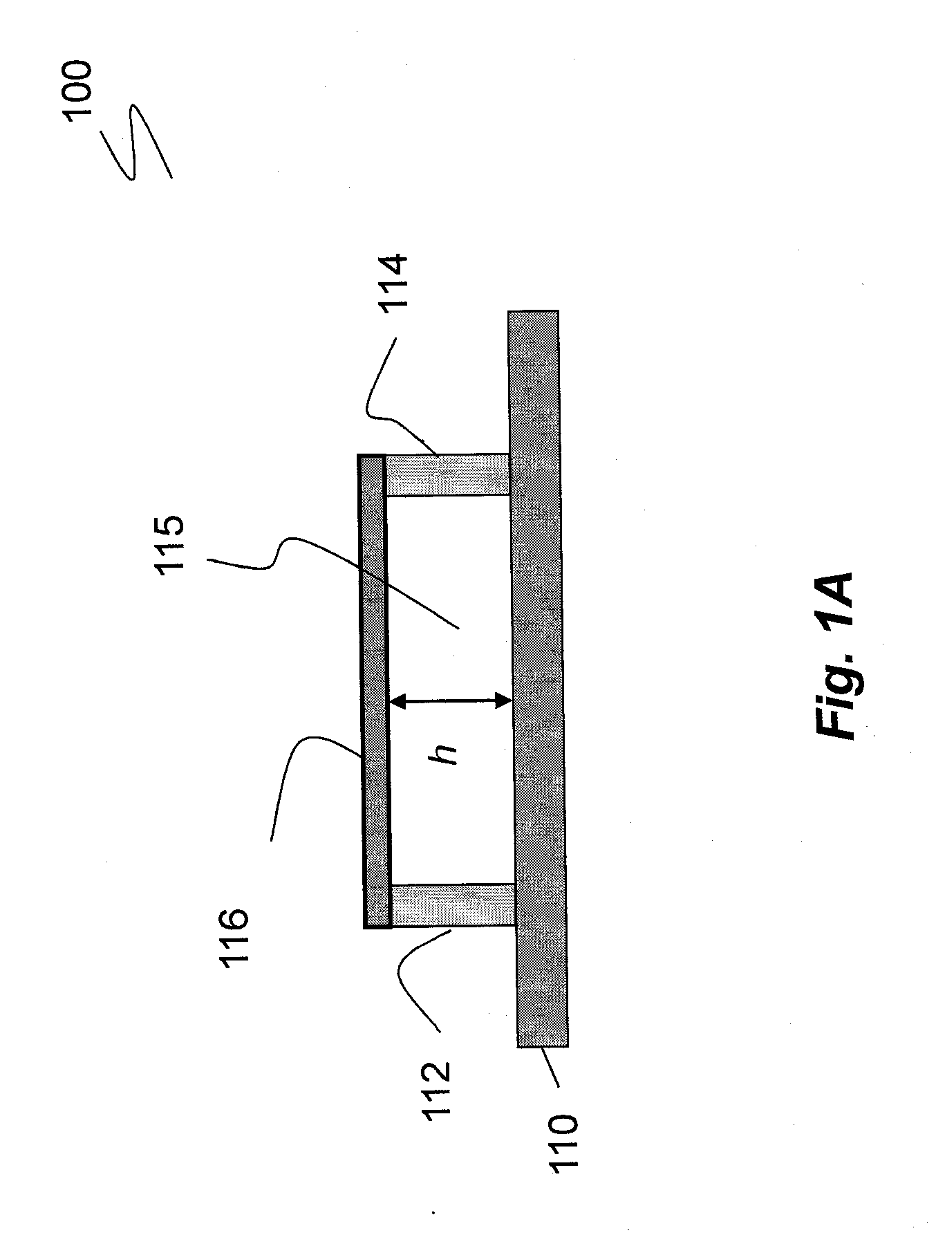
[0040]FIG. 1A is a schematic representation of a conventional MEMS device. MEMS 100 includes substrate 110 having supports 112 and 114. Supports 112 and 114 can be viewed as a plurality of ridges separated by gap 115. Supports 112 and 114 uphold layer 116. Gap 115 is defined by the separation distance between ridges 112 and by the height (h). Conventionally, layer 116 is defined by a metal layer and MEMS structure 100 is formed through photolithography as described above. As stated, the conventional processes lacked ability to produce MEMS devices over large areas and on flexible substrates.

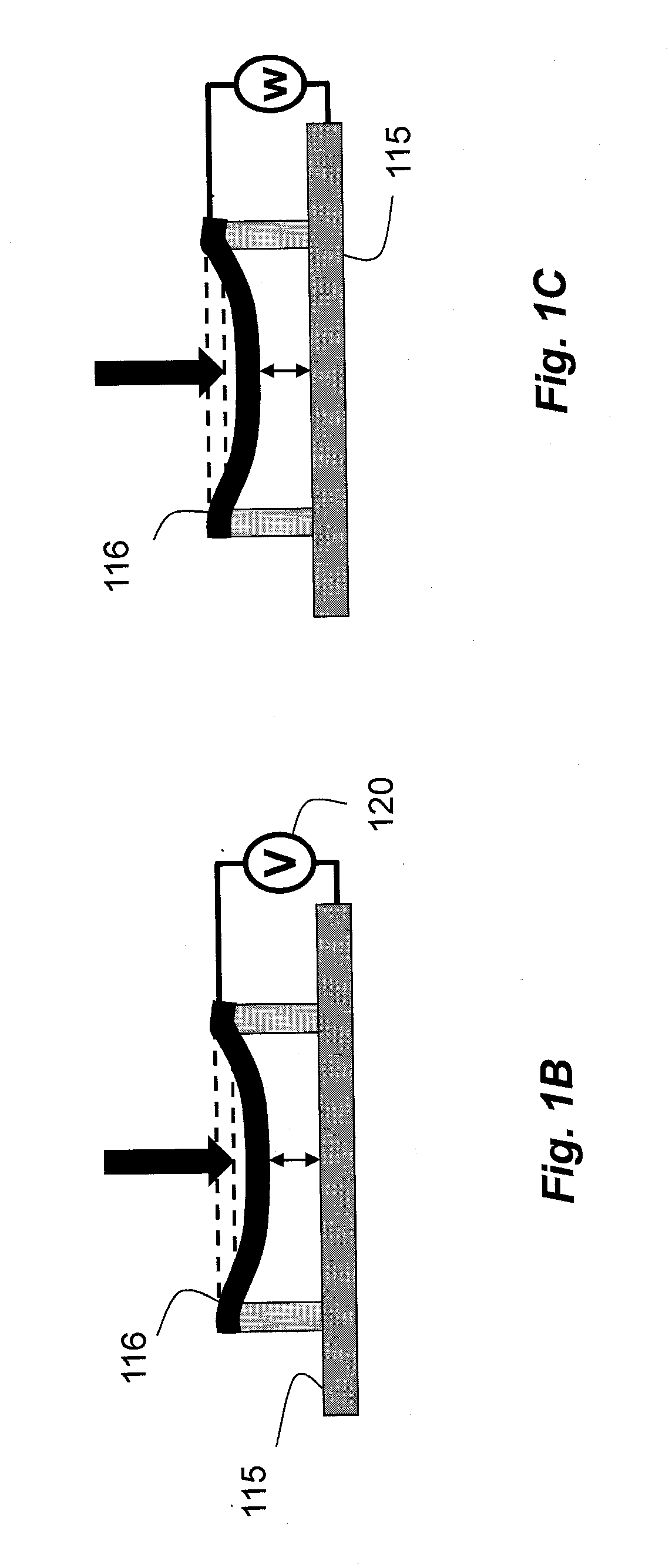
[0041]FIG. 1B shows an application of the MEMS device of FIG. 1A used as an actuator. In FIG. 1B, structure 100 is connected to voltage source 120 through substrate 115 and diaphragm 116 which act as electrodes. The bias provided by voltage source 120 creates an electrostatic force between electrode 115 and layer 116, causing the latter to act as a diaphragm by deflecting towards electrode 115. T...


PUM


Abstract

The disclosure is generally directed to fabrication steps, and operation principles for microelectromechanical (MEMS) transducers. In one embodiment, the disclosure relates to a texture morphing device. The texture morphing device includes: a plurality of supports arranged on a substrate to support a deformable mirror; an ITO layer; and a Distributed Bragg Reflector (DBR) layer. A pair of adjacent supports form a cavity with the ITO layer and the deformable mirror. When the height of the cavity changes responsive to an external pressure, the internal reflection within the cavity is changed. The change in the height of the cavity causes the exterior texture to morph. Similar principles are disclosed for constructing sensor and actuators.

Description

[0001]The application claims the filing-date priority of Provisional Application No. 61 / 251,255, filed Oct. 13, 2009, the disclosure of which is incorporated herein in its entirety; the application is also a continuation-in-part of U.S. patent application Ser. No. 12 / 537,424 filed Aug. 13, 2007; and is a continuation-in-part of application Ser. No. 12 / 636,757 filed Dec. 13, 2009. The disclosure of the foregoing applications are incorporated herein in their entirety for background information.BACKGROUND[0002]1. Field of the Invention[0003]The disclosure relates to a method and apparatus for forming microelectromechanical systems (“MEMS”) devices. More specifically, the disclosure relates to forming highly sensitive detection and actuation apparatus using, among others, contact transfer method described herein.[0004]2. Description of Related Art[0005]MEMS applied over large areas would enable applications in such diverse areas as sensor skins for humans and vehicles, phased array dete...

Claims


Application Information

Patent Timeline
IPC IPC(8): H01L29/84H01L21/02G02B26/08H01L21/66
CPCH01L51/5265B81C1/0046B81C1/00357H10K50/852
Inventor BULOVIC, VLADIMIRPACKARD, CORINNE E.WOOD, VANESSA C.
Owner MASSACHUSETTS INST OF TECH
Features
  • Generate Ideas
  • Intellectual Property
  • Life Sciences
  • Materials
  • Tech Scout
  • Unparalleled Data Quality
  • Higher Quality Content
  • 60% Fewer Hallucinations
Learn More