Monolithic ceramic electronic component and method for manufacturing the same

a technology of monolithic ceramics and electronic components, applied in the direction of fixed capacitor details, stacked capacitors, transportation and packaging, etc., can solve the problems of kirkendall voids in the plated layer and deterioration in product lifetime, and achieve the effect of effectively preventing the occurrence of kirkendall voids, reducing the diffusion of the main component metal of the plated layer in the internal electrode, and improving product lifetime in a load test environmen

Inactive Publication Date: 2011-10-20
MURATA MFG CO LTD
View PDF4 Cites 0 Cited by
  • Summary
  • Abstract
  • Description
  • Claims
  • Application Information

AI Technical Summary

Benefits of technology

[0015]A preferred embodiment of the present invention is more effective when the specific metal is Cu, and the metal defining the internal electrodes is Ni.
[0020]According to a preferred embodiment of the present invention, in a method for manufacturing a monolithic ceramic electronic component, the same or substantially the same metal that defines internal electrodes is uniformly distributed in a plated layer disposed directly on a surface at which the internal electrodes are exposed. Thus, the diffusion of the main component metal of the plated layer in the internal electrodes is reduced during heat treatment. This prevents the generation of Kirkendall voids in the plated layer, and accordingly, the product lifetime in a load test under a high temperature and high humidity environment is improved.
[0021]In particular, when the main component of the plated layer is Cu and the plated layer includes Ni, and the main component of the internal electrodes is Ni, the Ni in the plated layer can more effectively prevent the migration of diffusive Cu, thus more effectively preventing the occurrence of Kirkendall voids.
[0022]Furthermore, interfaces between the internal electrodes and the ceramic layers exposed at the end surfaces can be sealed more tightly by heat treatment. This effectively prevents water from entering the laminate, which ensures high reliability.

Problems solved by technology

However, in this method, a plating solution tends to enter the laminate from the side surfaces at which the internal electrodes are exposed.
When the laminate is heated at about 800° C. to remove water in the plating solution, Cu in a plated layer may be significantly diffused along the internal electrodes, causing Kirkendall voids in the plated layer.
A Kirkendall void having an opening on the surface of the plated layer allows water to enter the laminate, thus causing deterioration in product lifetime under high temperature and high humidity.

Method used


Image

  • Monolithic ceramic electronic component and method for manufacturing the same
  • Monolithic ceramic electronic component and method for manufacturing the same
  • Monolithic ceramic electronic component and method for manufacturing the same

Examples


first preferred embodiment

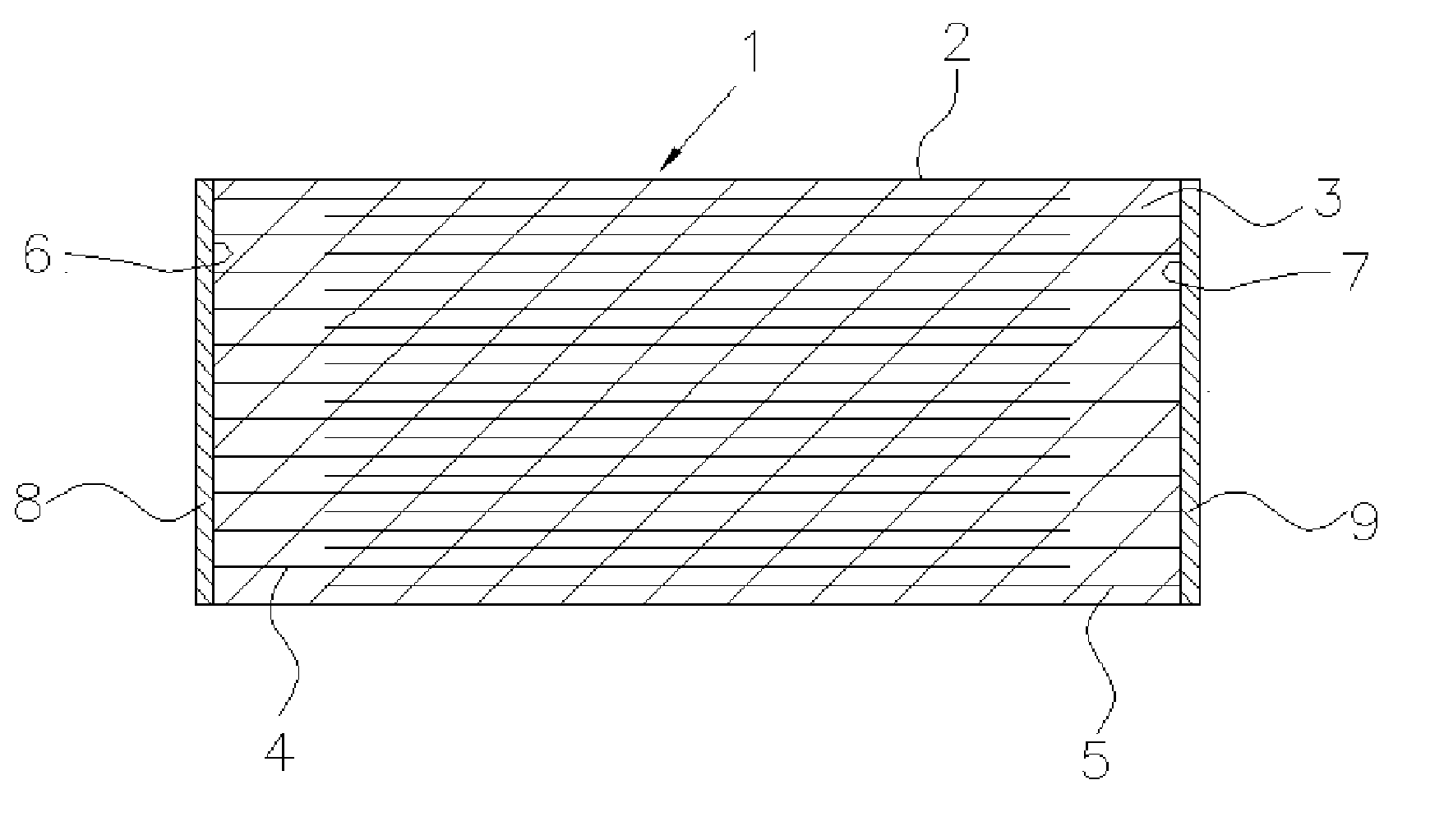
[0029]A monolithic ceramic electronic component 1 according to a first preferred embodiment of the present invention and a method for manufacturing the monolithic ceramic electronic component 1 are described below with reference to FIGS. 1 and 2.

[0030]As illustrated in the cross-sectional view of FIG. 1, the monolithic ceramic electronic component 1 includes a laminate 2, which includes laminated ceramic layers 3 and internal electrodes 4 and 5 alternately disposed between the ceramic layers 3. When the monolithic ceramic electronic component 1 is a monolithic ceramic capacitor, the ceramic layers 3 are composed of dielectric ceramic. An end of each of the internal electrodes 4 is exposed at an end surface 6 of the laminate 2. An end of each of the internal electrodes 5 is exposed at an end surface 7. External electrodes are formed on the end surfaces 6 and 7 to electrically connect the corresponding ends of the internal electrodes 4 and 5.

[0031]The external electrodes include first...

second preferred embodiment

[0045]FIG. 4 is a cross-sectional view of a monolithic ceramic electronic component 51 according to a second preferred embodiment of the present invention. A method for manufacturing the monolithic ceramic electronic component 51 is described below.

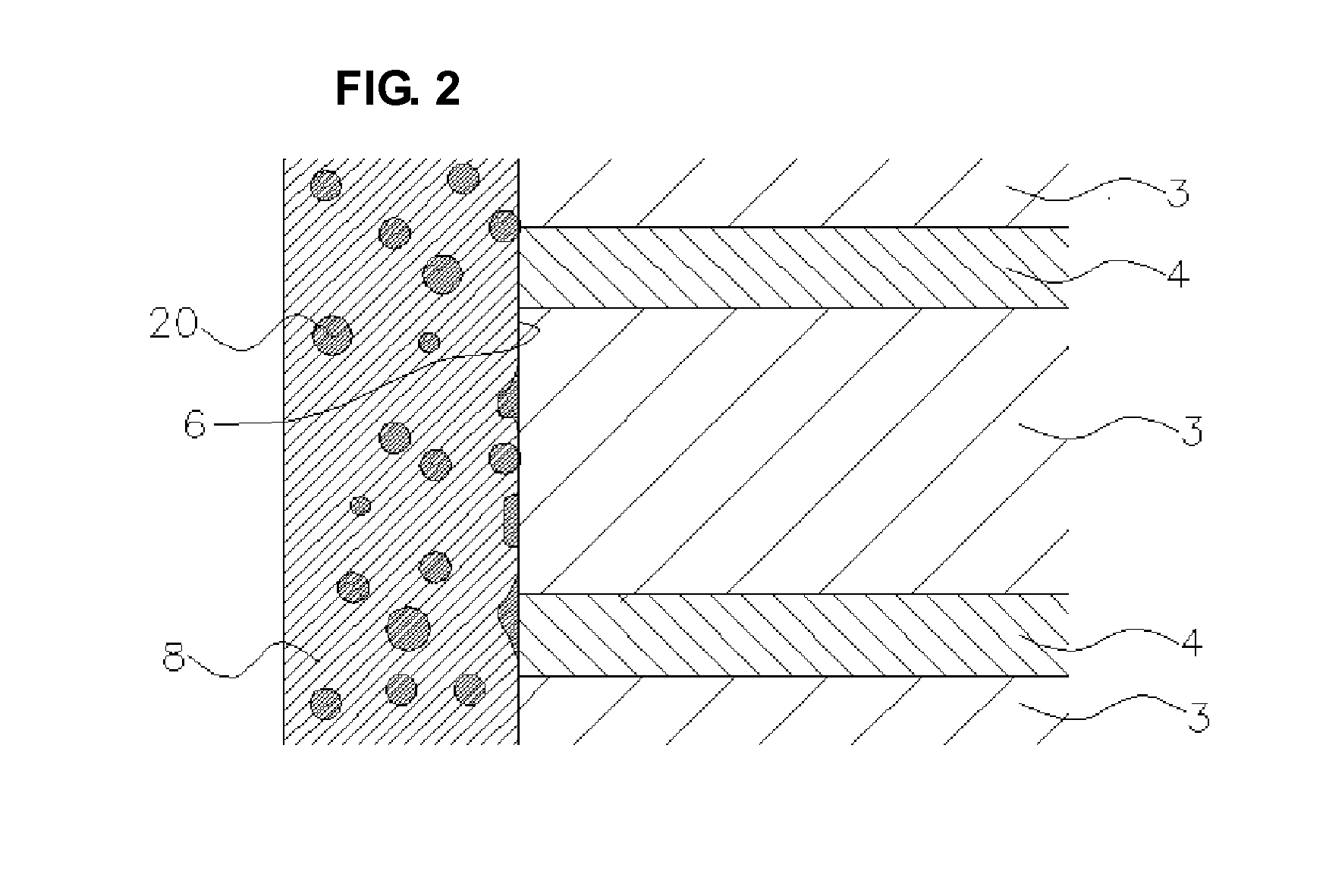
[0046]First, a laminate 2 is prepared as in the first preferred embodiment. First plated layers 8 and 9 are formed as in the first preferred embodiment on end surfaces 6 and 7 of the laminate 2 at which internal electrodes 4 and 5 are exposed. The first plated layers 8 and 9 are formed of a metal different from that of the internal electrodes 4 and 5.

[0047]The second preferred embodiment is different from the first preferred embodiment in that second plated layers 10 and 11 primarily composed of the same or substantially the same metal that defines the internal electrodes 4 and 5 are formed on the first plated layers 8 and 9 and that the laminate 2 is subsequently heat-treated at a temperature of at least about 800° C. The heat treatment ...

example 1

[0063]A laminate for use in a monolithic ceramic capacitor was prepared as a laminate of a monolithic ceramic electronic component. The laminate included ceramic layers made of barium titanate-based dielectric ceramic and internal electrodes primarily made of Ni. The laminate had a length of about 1.9 mm, a width of about 1.05 mm, and a height of about 1.05 mm. Each of the ceramic layers had a thickness of about 2.0 μm. The distance between adjacent internal electrodes on a surface at which the internal electrodes were exposed was about 4.0 μm.

[0064]Five hundred laminates were charged in a horizontal rotating barrel having a volume of about 290 mL. A hundred milliliters of electroconductive media having a diameter of about 1.3 mm were charged in the barrel. The rotating barrel was immersed in a Cu / Ni alloy plating bath controlled at a pH of about 8.7 and a temperature of about 25° C. An electric current was applied at a density of about 0.50 A / dm2 for a predetermined period of time ...


PUM

PropertyMeasurementUnit
temperatureaaaaaaaaaa
thicknessaaaaaaaaaa
distanceaaaaaaaaaa

Abstract

A method for manufacturing a monolithic ceramic electronic component includes a plating substep of depositing precipitates primarily composed of a specific metal on an end of each of internal electrodes exposed at a predetermined surface of a laminate and growing the precipitates to coalesce into a continuous plated layer, wherein the specific metal is different from that of the internal electrodes, and the same or substantially the same metal that defines the internal electrodes is distributed throughout the plated layer.

Description

BACKGROUND OF THE INVENTION[0001]1. Field of the Invention[0002]The present invention relates to a monolithic ceramic electronic component and a method for manufacturing the monolithic ceramic electronic component and, in particular, to a monolithic ceramic electronic component in which external electrodes are directly formed on the surface of a laminate by plating and a method for manufacturing the monolithic ceramic electronic component.[0003]2. Description of the Related Art[0004]As illustrated in FIG. 5, a monolithic ceramic electronic component 101, such as a monolithic ceramic capacitor, includes a laminate 102, which includes ceramic layers 103 and internal electrodes 104 and 105 alternately disposed between the ceramic layers 103. An end of each of the internal electrodes 104 is exposed at an end surface 106 of the laminate 102. An end of each of the internal electrodes 105 is exposed at an end surface 107. External electrodes are provided on the end surfaces 106 and 107 to ...

Claims


Application Information

Patent Timeline
Patent Type & Authority Applications(United States)
IPC IPC(8): B05D5/12
CPCB32B18/00C04B2237/346C04B2237/704H01C1/142Y10T428/265H01G4/232H01G4/30C04B2237/66C04B2237/68H01C7/008Y10T428/31678
Inventor IWANAGA, TOSHIYUKIMOTOKI, AKIHIROOGAWA, MAKOTOKAWASAKI, KENICHITAKEUCHI, SHUNSUKINISHIHARA, SEIICHIMATSUMOTO, SHUJI
Owner MURATA MFG CO LTD
Why Eureka
Try Eureka