Semiconducting composition

a composition and semiconductor technology, applied in the field of semiconductor compositions, can solve the problems of high cost of silicon-based tft circuits, and high cost of silicon-based tft circuits, and achieve good film-forming properties and high mobility

Active Publication Date: 2011-10-27
SAMSUNG ELECTRONICS CO LTD
View PDF7 Cites 19 Cited by
  • Summary
  • Abstract
  • Description
  • Claims
  • Application Information

AI Technical Summary

Benefits of technology

[0006]The present application discloses, in various embodiments, semiconducting compositions comprising a non-amorphous semiconductor material and a molecular glass. Electronic devices,

Problems solved by technology

TFT circuits using current mainstream silicon technology are too costly for some applications, particularly for large-area electronic devices such as backplane switching circuits for displays (e.g., active matrix liquid crystal monitors or televisions) where high switching speeds are not essential.
The high costs of silicon-based TFT circuits are primarily

Method used


Image

  • Semiconducting composition
  • Semiconducting composition
  • Semiconducting composition

Examples


Embodiment Construction

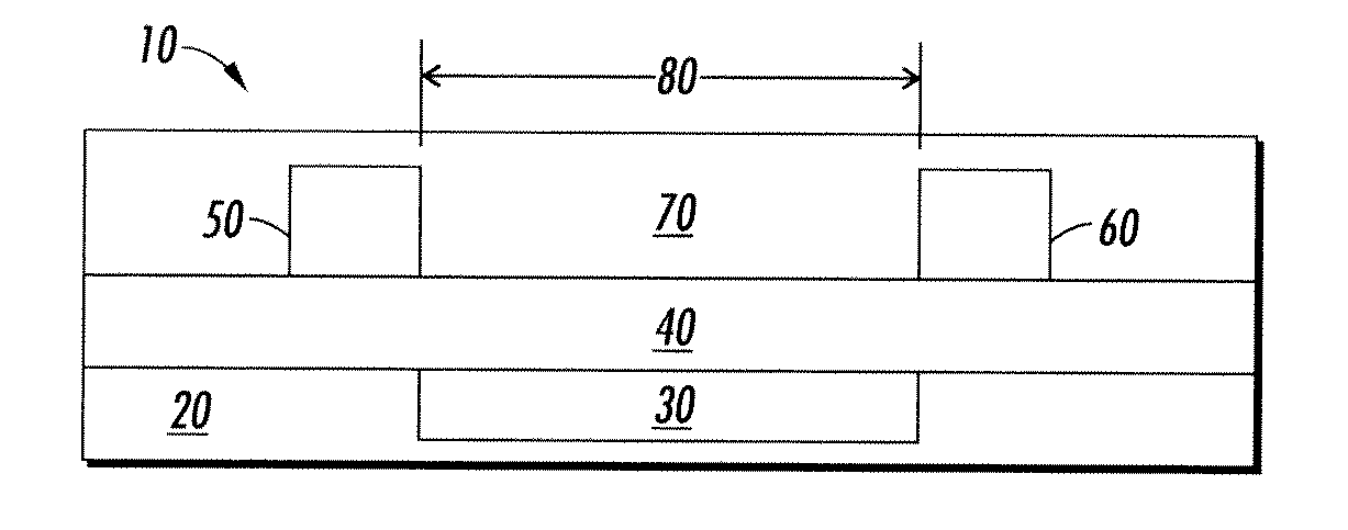
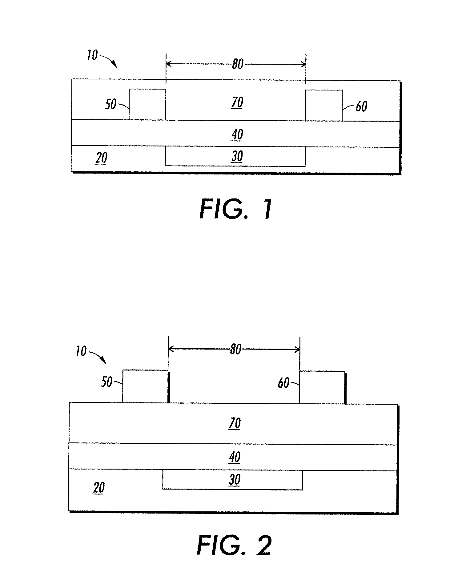
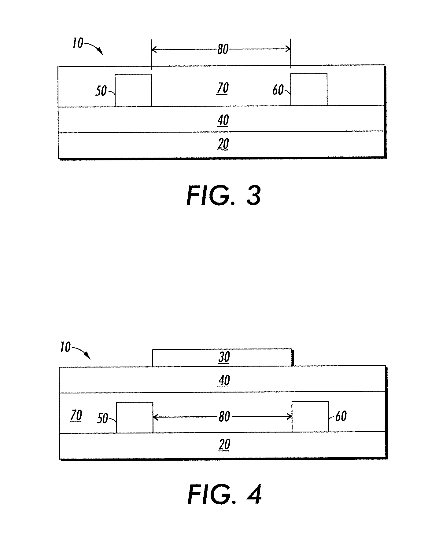
[0031]A more complete understanding of the components, processes, and apparatuses disclosed herein can be obtained by reference to the accompanying drawings. These figures are merely schematic representations based on convenience and the ease of demonstrating the present disclosure, and are, therefore, not intended to indicate relative size and dimensions of the devices or components thereof and / or to define or limit the scope of the exemplary embodiments.

[0032]Although specific terms are used in the following description for the sake of clarity, these terms are intended to refer only to the particular structure of the embodiments selected for illustration in the drawings, and are not intended to define or limit the scope of the disclosure. In the drawings and the following description below, it is to be understood that like numeric designations refer to components of like function.

[0033]The modifier “about” used in connection with a quantity is inclusive of the stated value and has...


PUM


Abstract

The present application discloses, in various embodiments, semiconducting layer compositions comprising a non-amorphous semiconductor material and a molecular glass. Electronic devices, such as thin-film transistors, are also disclosed. The semiconducting layer compositions exhibit good film-forming properties and high mobility.

Description

BACKGROUND[0001]The present disclosure relates to semiconducting compositions for making semiconducting layers useful in electronic devices, such as thin film transistors (TFTs). Among other advantages, the semiconducting layers exhibit high field effect mobility and good film-forming properties.[0002]Thin film transistors (TFTs) are critical components in modern-age electronics, including, for example, sensors, image scanners, and electronic display devices. TFT circuits using current mainstream silicon technology are too costly for some applications, particularly for large-area electronic devices such as backplane switching circuits for displays (e.g., active matrix liquid crystal monitors or televisions) where high switching speeds are not essential. The high costs of silicon-based TFT circuits are primarily due to the use of capital-intensive silicon manufacturing facilities as well as complex high-temperature, high-vacuum photolithographic fabrication processes under strictly c...

Claims


Application Information

Patent Timeline
IPC IPC(8): H01B1/12
CPCH01L51/005H01L51/0094H01L51/0074H01L51/0073H10K85/60H10K85/6576H10K85/6574H10K85/40
Inventor WU, YILIANGLIU, PINGWIGGLESWORTH, ANTHONY JAMESHU, NAN-XING
Owner SAMSUNG ELECTRONICS CO LTD
Why Eureka
Try Eureka