
Semiconductor device and method of manufacturing the same

a technology of semiconductor devices and dielectric films, applied in semiconductor devices, electrical equipment, transistors, etc., can solve the problems of reducing reliability, reducing the threshold voltage and the mobility of channel carriers, and reducing oxygen vacancies and defect density, so as to achieve effective control of oxygen vacancies and defects of high-k gate dielectric films, and continuous scaling

Active Publication Date: 2011-10-27
INST OF MICROELECTRONICS CHINESE ACAD OF SCI
View PDF3 Cites 13 Cited by
  • Summary
  • Abstract
  • Description
  • Claims
  • Application Information

AI Technical Summary

Benefits of technology

[0008]Through the present invention, the oxygen vacancies and defects of high-k gate dielectric film may be alleviated by the catalyzing decomposition of the catalyzing layer to oxygen molecules at lower temperature, and the growth of low dielectric constant SiOx interface layer caused by the traditional PDA high temperature process may be prevented, and thus EOT of the entire gate dielectric layer may be controlled effectively, and the MOS device may be scaled continuously.

Problems solved by technology

However, there exists serious problems caused by oxygen vacancies in the Hf-base high-k gate dielectric film, such as degradation of the threshold voltage and the mobility of channel carriers, and reduction of reliability, etc.
Therefore, it has become a challenge to alleviate oxygen vacancies and defect density in the high-k gate dielectric film.
1. In the process for manufacturing an MOS device with a high-k metal structure in prior art, the high-k film layer are typically formed by a chemical method (atomic layer deposition or metal organic chemical vapor deposition), which may cause more defects and charge traps, and insufficient density and compactness of the high-k film.
It disadvantageously leads to increase of EOT for the whole gate structure and degradation of the overall performance for the MOS device.
However, this method only allows less oxygen to diffuse into the high-k gate dielectric film, which may partially supplement the oxygen vacancies and defect traps in the high-k gate dielectric film, and there is still a lot of oxygen vacancies and defect traps in the film.

Method used


Image

  • Semiconductor device and method of manufacturing the same
  • Semiconductor device and method of manufacturing the same
  • Semiconductor device and method of manufacturing the same

Examples


Embodiment Construction

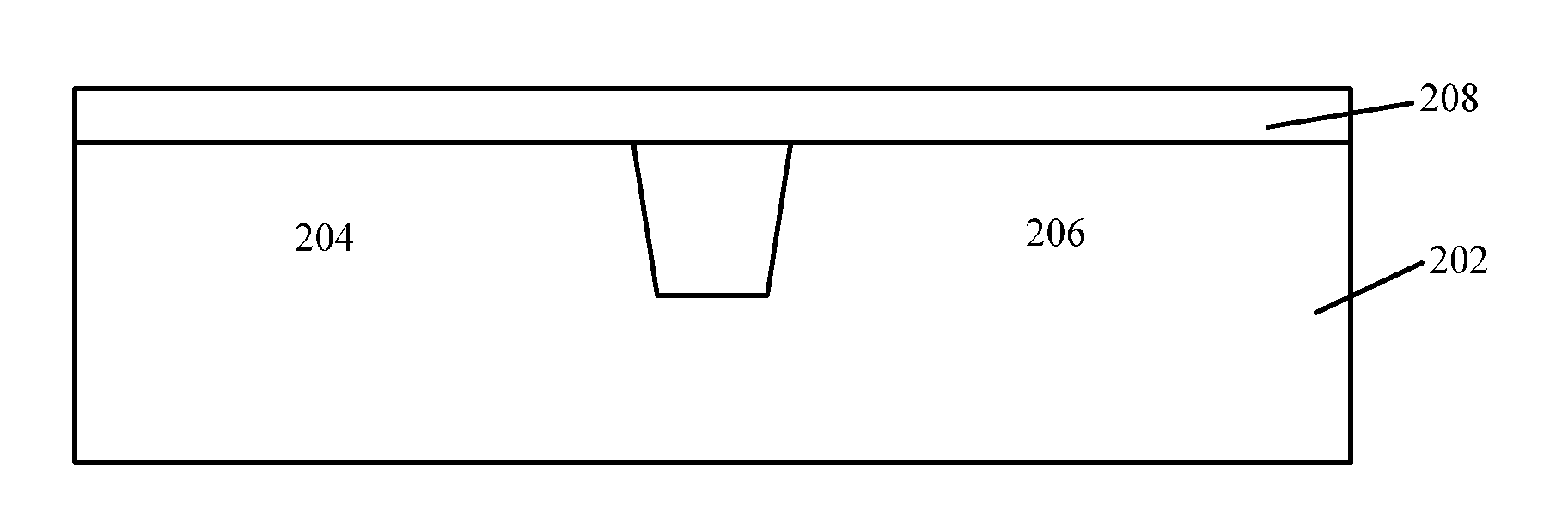
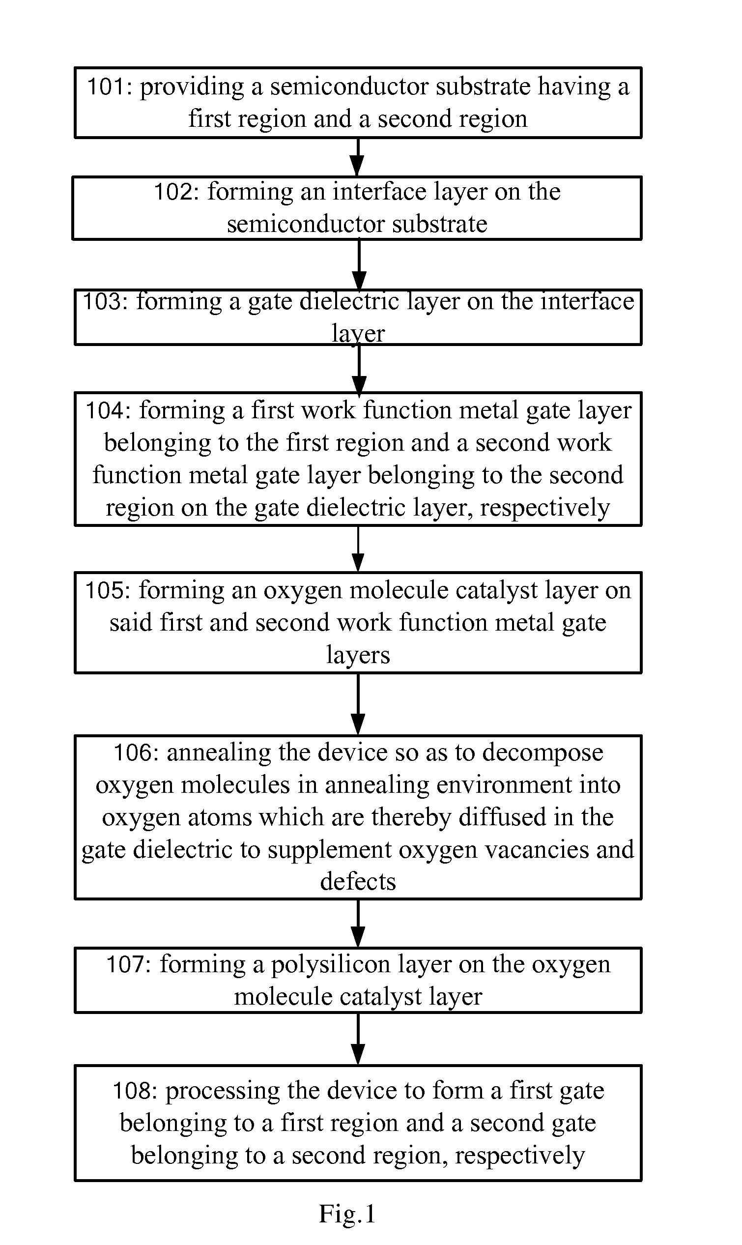
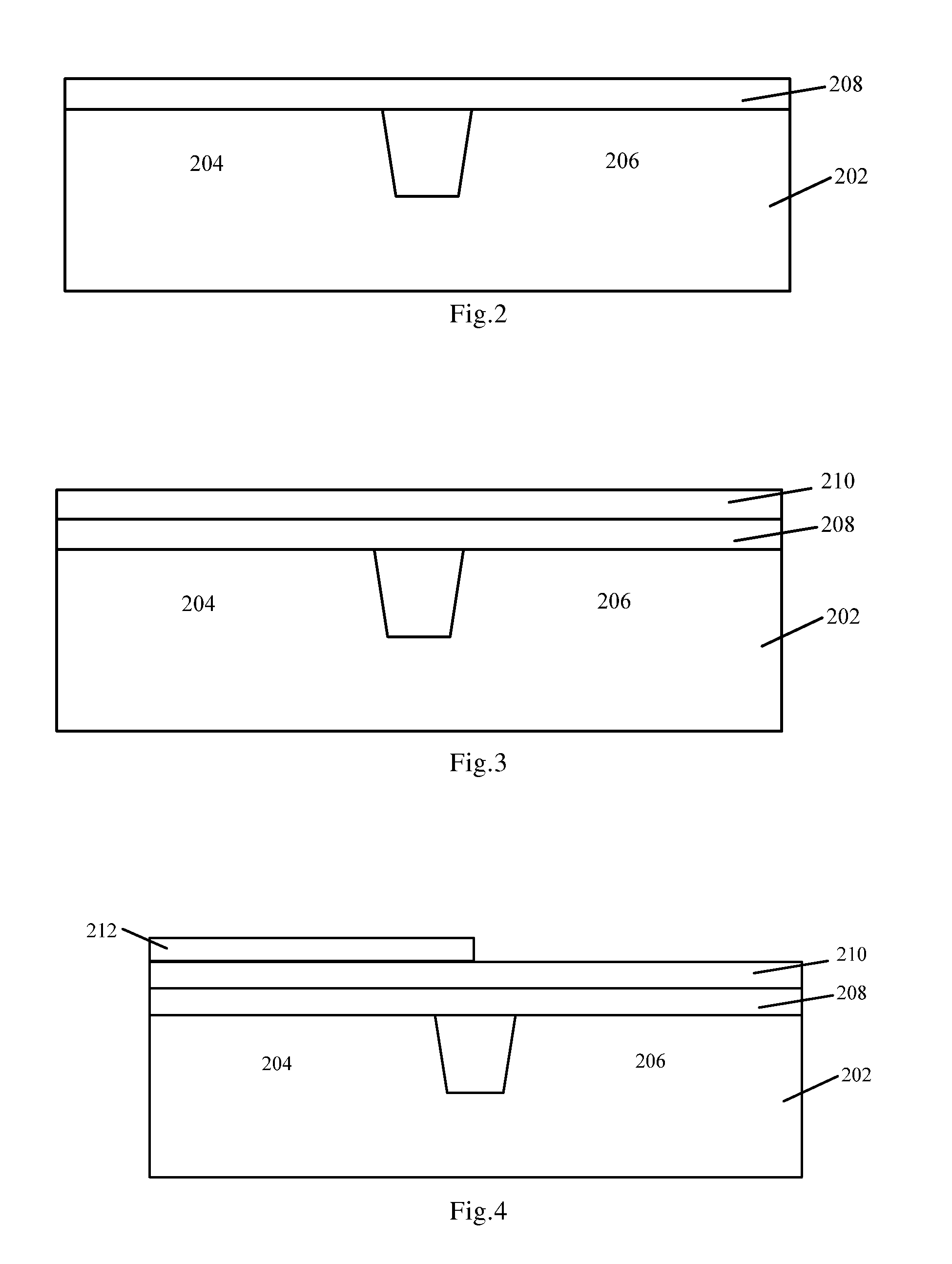
[0011]The present invention generally relates to a method of manufacturing a semiconductor device, and more particularly, to a method of alleviating oxygen vacancies in a high-k gate dielectric layer. The following disclosure provides a plurality of different embodiments or examples to achieve different structure of the present invention. To simplify the disclosure of the present invention, description of the components and arrangements of specific examples is given below. Of course, they are only illustrative and not limiting the present invention. Moreover, in the present invention, reference numbers and / or letters may be repeated in different embodiments. Such repetition is for the purposes of simplification and clearness, and does not denote the relationship between respective embodiments and / or arrangements being discussed. In addition, the present invention provides various examples for specific process and materials. However, it is obvious for a person of ordinary skill in th...


PUM


Abstract

The present invention relates to a method of manufacturing a semiconductor device. After depositing the metal gate electrode material, a layer of oxygen molecule catalyzing layer having a catalyzing function to the oxygen molecules is deposited, and afterwards, a low-temperature PMA annealing process is used to decompose the oxygen molecules in the annealing atmosphere into more active oxygen atoms. These oxygen atoms are diffused into the high-k gate dielectric film through the metal gate to supplement the oxygen vacancies in the high-k film, in order to alleviate oxygen vacancies in the high-k film and improve the quality of the high-k film. According to the present invention, the oxygen vacancies and defects of high-k gate dielectric film will be alleviated, and further, growth of SiOx interface layer having a low dielectric constant caused by the traditional PDA high temperature process may be prevented. Thereby, the EOT of the entire gate dielectric layer may be effectively controlled, and the MOS device may be continuously scaled. Meanwhile, the present invention further provides a semiconductor device obtained according to the above-mentioned method.

Description

FIELD OF THE INVENTION[0001]The present invention generally relates to a semiconductor device and a method of manufacturing the same, and more specifically, to a method of manufacturing a semiconductor device and the same device for alleviating oxygen vacancies in a high-k gate dielectric layer.BACKGROUND OF THE INVENTION[0002]With the development of the semiconductor industry, integrated circuits with higher performance and more powerful functions require greater element density. Thus, the sizes of the components need to be scaled further. The application of the core technology for the 32 / 22 nanometer process has been the inevitable trend for the development of integrated circuits, and is also one of the tasks that major international semiconductor companies and institutions compete to develop. Study on CMOS device gate engineering with the “high-k / metal gate” as the core technology is the most representative core process in 32 / 22 nanometer technology, and relevant research on mate...

Claims


Application Information

Patent Timeline
IPC IPC(8): H01L27/088H01L21/336
CPCH01L21/28176H01L21/823857H01L29/4916H01L29/517H01L29/4975H01L29/513H01L29/4966
Inventor WANG, WENWUCHEN, SHIJIEWANG, XIAOLEIHAN, KAICHEN, DAPENG
Owner INST OF MICROELECTRONICS CHINESE ACAD OF SCI
Learn More