Semiconductor device, and manufacturing method of semiconductor device
Active Publication Date: 2011-11-03
RENESAS ELECTRONICS CORP
View PDF10 Cites 31 Cited by
Summary
Abstract
Description
Claims
Application Information
AI Technical Summary
This helps you quickly interpret patents by identifying the three key elements:
Problems solved by technology
Method used
Benefits of technology
Benefits of technology
[0015]An improvement is made in the reliability of a semiconductor device having a slit made over a main surface of a semiconductor substrate so as to surround an element formation region.
Problems solved by technology
In a dicing step of cutting a semiconductor wafer into the form of chips, there is caused a problem that various films thereon are peeled or cracked, examples of the films including a low-k film (an insulating film having a dielectric constant of 3.5 or less) comprised of an interlayer dielectric, a BPSG (boron-doped phosphorsilicate glass) film, which is smaller in mechanical strength than siliconoxide films, and a siliconnitride film, which is higher in film stress than siliconoxide films.
When the water invades the element formation region, there is caused, for example, a problem that in a reliability test for the semiconductor device, the copperinterconnection in the element formation region corrodes so that the reliability of the semiconductor device deteriorates.
Method used
Image
Click on the blue label to locate the original text in one second.
Reading with bidirectional positioning of images and text.
Examples
first embodiment
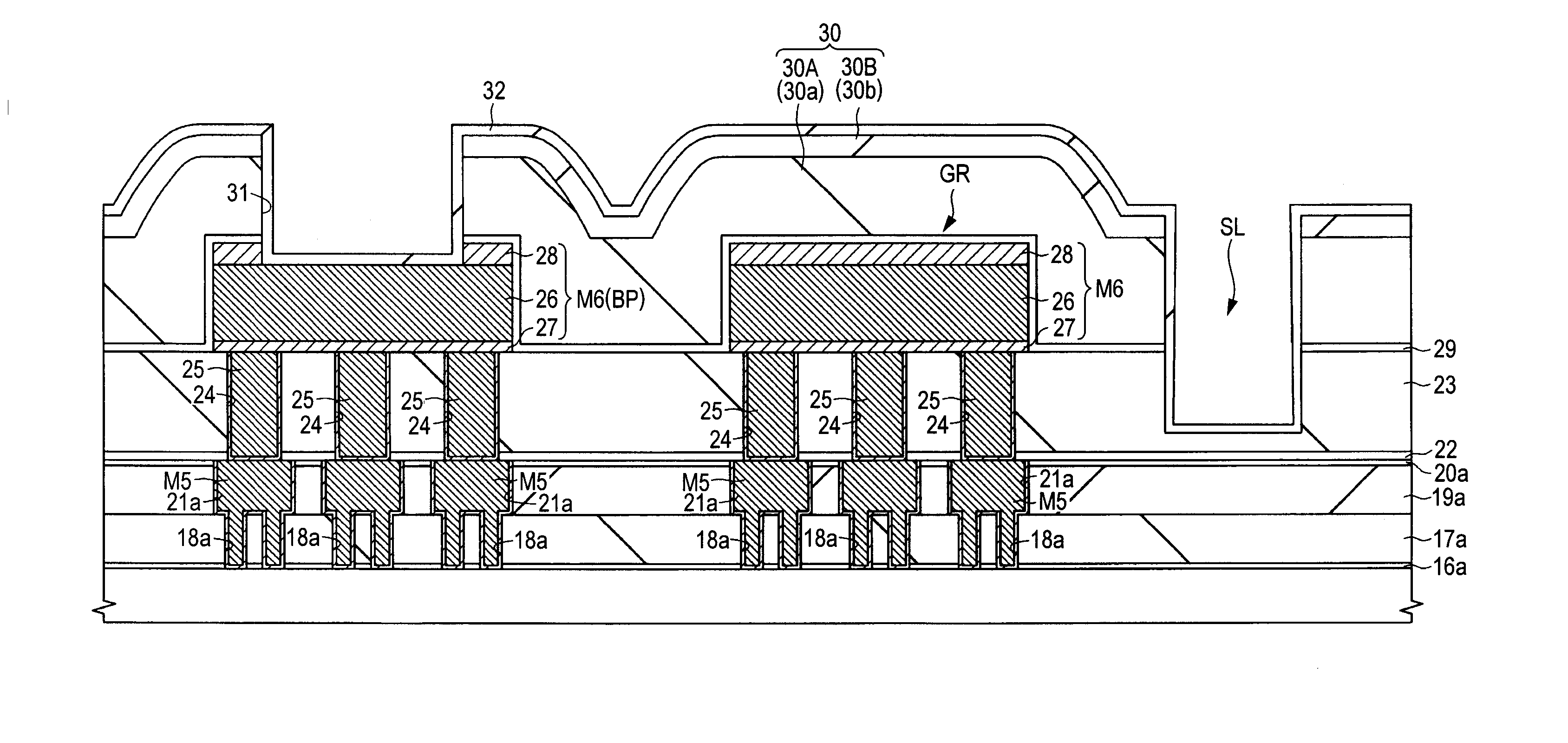
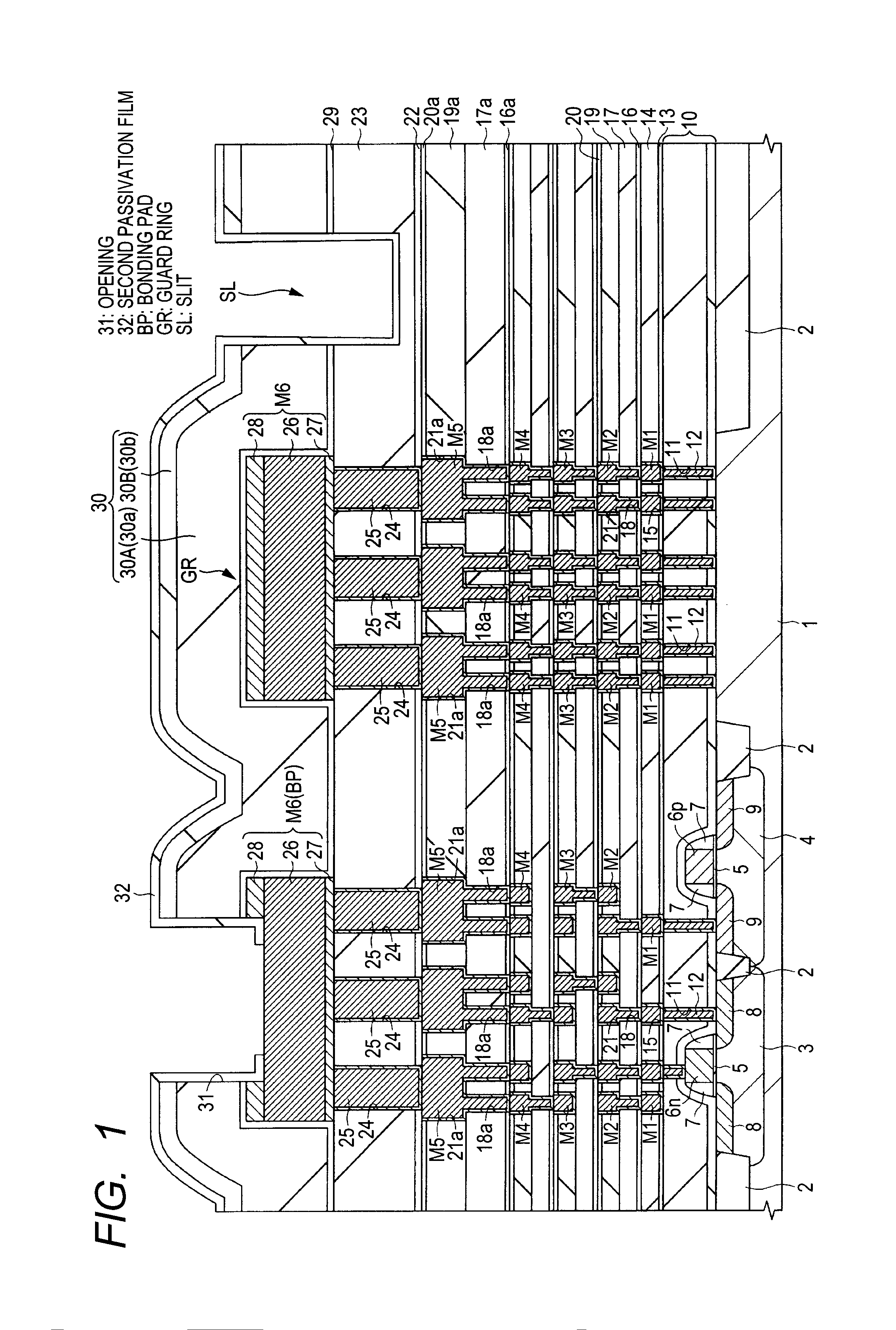
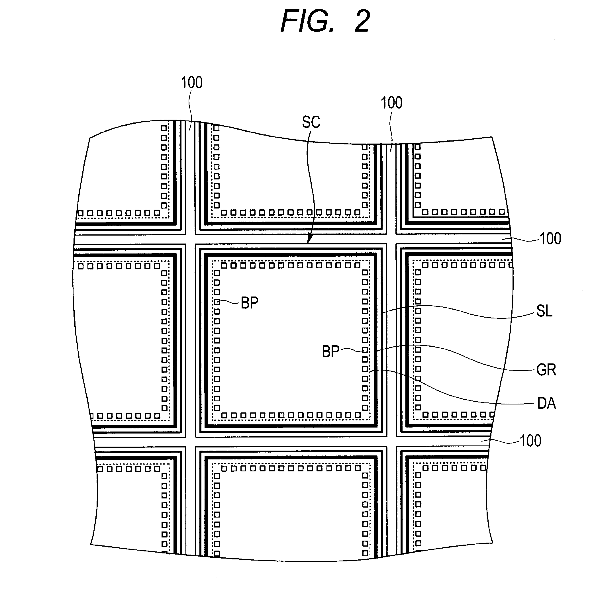
[0047]With reference to FIGS. 1 and 2, a semiconductor device according to the first embodiment is described hereinafter. FIG. 1 is a partial sectional view of the semiconductor device, and FIG. 2 is a partial plan view of the device.
[0048]As illustrated in FIG. 1, a semiconductor device comprised of various desired semiconductor elements is formed in / over a main surface of a semiconductor substrate (semiconductor wafer worked in the form of a circular thin plate) made of a silicon monocrystal, so as to be assigned to each of divided semiconductor chips in the main surface. Examples of the semiconductor elements include CMOS (complementary metaloxide semiconductor) devices, resistance elements, and capacitance elements. In the first embodiment, CMOS devices are given as examples. A p-channel MISFET which configures a CMOS device is abbreviated as a pMIS, and an n-channel MISFT which configures a CMOS is abbreviated as an nMIS.
[0049]In each element formation region of the semiconduc...
second embodiment
[0092]In the first embodiment, the inner walls (the side surfaces and the bottom surface) of the slit SL made to surround the circumference of the guard ring GR are covered with the second passivation film 32, thereby preventing water from invading the element formation region through the slit SL. Moreover, the side surface of the opening 31, which is made to make the upper surface of the sixth-layer interconnection M6 used for the bonding pads BP naked, is covered with the second passivation film 32, thereby preventing the TiN film 28 from being made naked, so as to prevent the first passivation film 30 from being cracked by an expansion in the volume of the TiN film 28 through oxidization. In this way, the invasion of water into the element formation region through cracks is prevented.
[0093]In the second embodiment, a sixth-layer interconnection which is an interconnection of a top layer is covered with a first passivation film in the same way as in the first embodiment; however, ...
third embodiment
[0107]A semiconductor device according to present the third embodiment is described with reference to FIGS. 16 and 17.
[0108]A description is first made about an example of the semiconductor device according to the third embodiment with reference to FIG. 16, which is a partial sectional view of this device example and illustrates upper-layer interconnections (corresponding to the above-mentioned fifth- and sixth-layer interconnections M5 and M6) in an element formation region and a slit region of the device example.
[0109]As illustrated in FIG. 16, a sixth-layer interconnection M6 is covered with an insulating film 29 for bonding, and a first passivation film 30. The bonding insulating film 29 is, for example, a silicon oxide film formed by plasma CVD, and is laid to prevent the first passivation film 30 from being peeled. The thickness thereof is, for example, about 70 nm.
[0110]The first passivation film 30 is a laminated film comprised of a lower-layer passivation film 30a and an up...
PUM
Abstract
Provided is a technique capable of improving the reliability of a semiconductor device having a slit made over a main surface of a semiconductor substrate, so as to surround each element formation region. In the technique, a second passivation film covers the side surface of an opening made to make the upper surface of a sixth-layer interconnection M6 used for bonding pads naked, and the inner walls (the side surfaces and the bottom surface) of a slit made to surround the circumference of a guard ring and made in a first passivation film, an insulating film for bonding, and an interlayer dielectric, so as to cause the bottom thereof not to penetrate through a barrier insulating film.
Description
CROSS-REFERENCE TO RELATED APPLICATIONS[0001]The disclosure of Japanese Patent Application No. 2010-103362 filed on Apr. 28, 2010 including the specification, drawings and abstract is incorporated herein by reference in its entirety.BACKGROUND[0002]The present invention relates to a semiconductor device, and a manufacturing method of the same, in particular, semiconductor device having a slit made over a main surface of a semiconductor substrate so as to surround an element formation region for the purpose of preventing an interlayer dielectric, an interconnection and some other from being peeled or cracked, and a method useful for manufacturing the device.[0003]For example, Japanese Unexamined Patent Publication No. 2007-115988 (Patent document 1) discloses a semiconductor device having the following members: an interlayer dielectric in which a first non-low-k film having a dielectric constant larger than 3.5, a low-k film having a dielectric constant of 3.5 or less, and a second n...
Claims
Application Information
Patent Timeline
Application Date:The date an application was filed.
Publication Date:The date a patent or application was officially published.
First Publication Date:The earliest publication date of a patent with the same application number.
Issue Date:Publication date of the patent grant document.
PCT Entry Date:The Entry date of PCT National Phase.
Estimated Expiry Date:The statutory expiry date of a patent right according to the Patent Law, and it is the longest term of protection that the patent right can achieve without the termination of the patent right due to other reasons(Term extension factor has been taken into account ).
Invalid Date:Actual expiry date is based on effective date or publication date of legal transaction data of invalid patent.

