

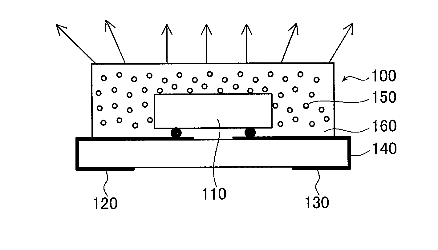
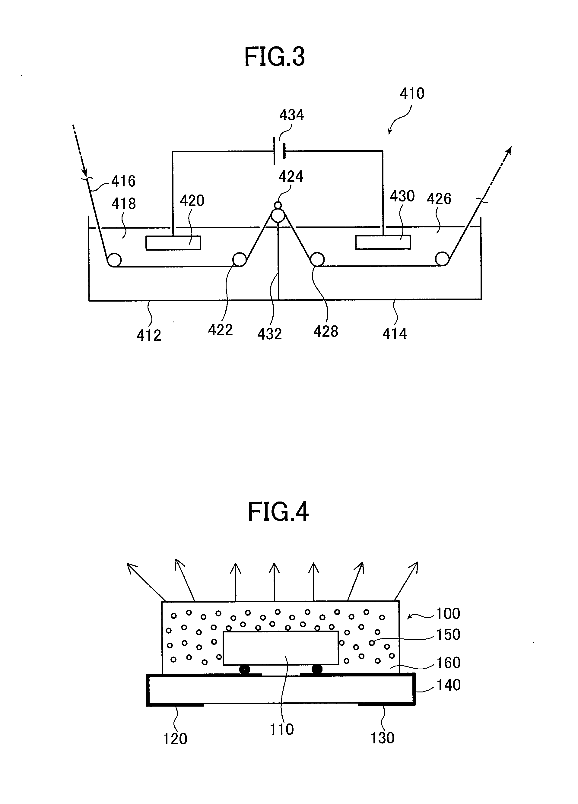
Insulated light-reflective substrate
a technology of light-reflective substrates and insulating layers, which is applied in the field of light-reflective substrates, can solve the problems of reducing the luminous efficacy and achieve the effect of reducing the cos
- Summary
- Abstract
- Description
- Claims
- Application Information
AI Technical Summary
Benefits of technology
Problems solved by technology
Method used
Image

Examples
examples
[0232]The present invention is illustrated by way of the following examples, to which the present invention is in no way limited.
examples 9 to 11
[0249]An aluminum alloy substrate fabricated in accordance with Example 4 was rolled to a thickness of 0.8 mm to use the resultant plate as a clad material, and ingots of the alloys A to C as set forth in Table 2 below were used as core materials. The clad material and each core material were stacked together, with a brazing material being sandwiched between them, and subjected as such to heat treatment in a furnace at 500° C. for three hours. The stacks were each hot rolled to bond the materials together by compression so as to fabricate the substrates of Examples 9 to 11.
[0250]The substrates thus fabricated were subjected to the same graining treatment and anodizing treatment as Example 1 to obtain insulated light-reflective substrates each having an anodized film (45 μm thick) on the surface of the substrate.
examples 15 to 17
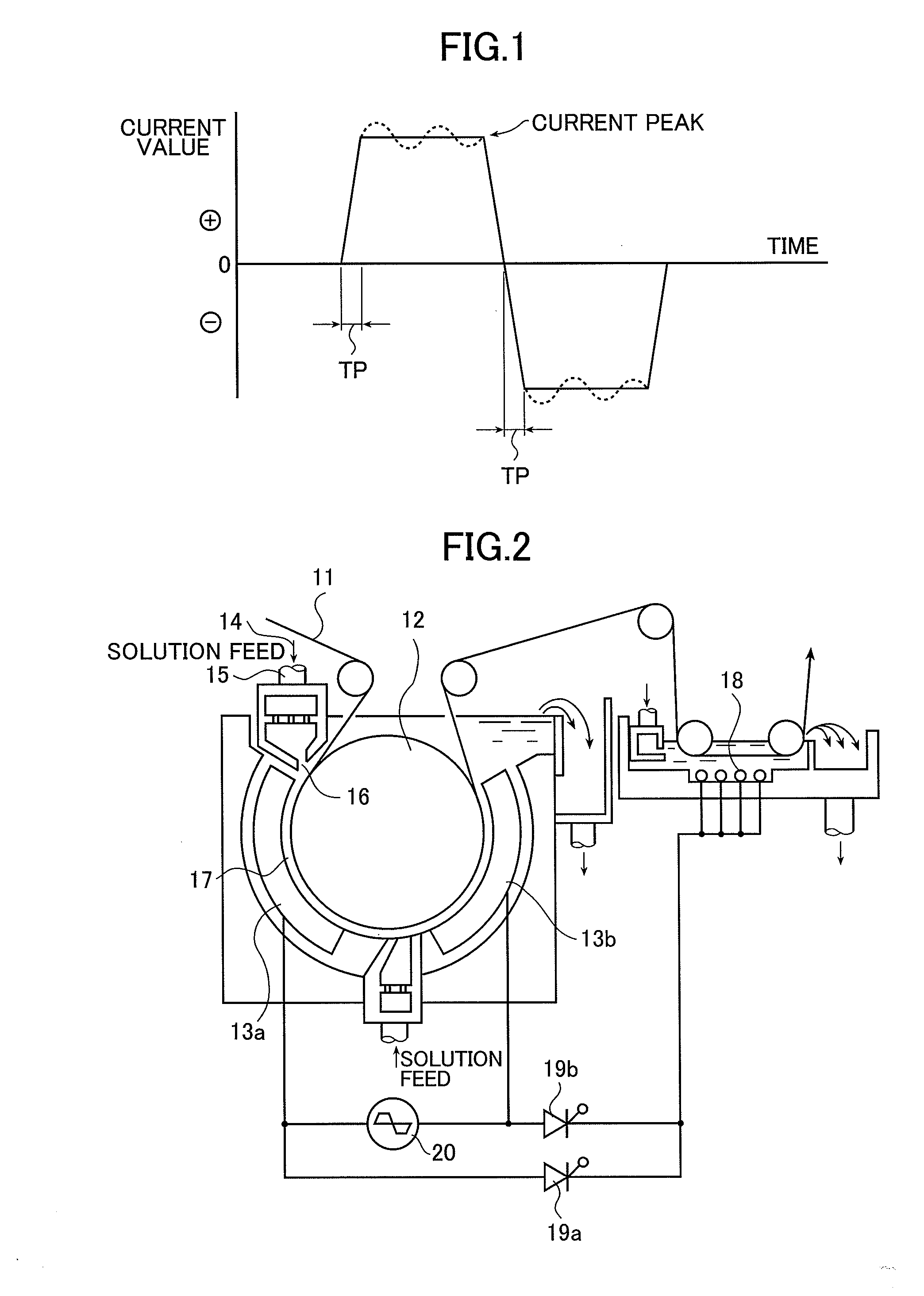
[0258]In each of Examples 15 to 17, the alloy ingot of Example 4 was used to fabricate a substrate, and the substrate was subjected to the same graining treatment as that carried out by the above treatments (a) to (f). In addition, each substrate was successively subjected to anodizing treatment with sulfuric acid and anodizing treatment with boric acid in this order under the conditions as described below to obtain an insulated light-reflective substrate.
[0259]Using sulfuric acid as an electrolyte solution, anodization was conducted for eight hours for Example 15, and for five hours for Examples 16 and 17 under such conditions that the sulfuric acid concentration was 30 g / L, the temperature was 17° C., and the voltage was 25 V. Subsequently, each substrate was rinsed with a spray of water.
[0260]The thickness of the anodized film as formed by the anodizing treatment with sulfuric acid was 45 μm in Example 15, and 25 μm in each of Examples 16 and 17.
[0261]In an aqueous solution at a ...
PUM
| Property | Measurement | Unit |
|---|---|---|
| Length | aaaaa | aaaaa |
| Fraction | aaaaa | aaaaa |
| Fraction | aaaaa | aaaaa |
Abstract
Description
Claims
Application Information