Semiconductor device having a buried gate that can realize a reduction in gate-induced drain leakage (GIDL) and method for manufacturing the same

a semiconductor device and drain leakage technology, applied in the field of semiconductor devices, can solve the problems of increasing the junction leakage current, reducing the channel length and becoming more and more difficult to achieve the appropriate threshold voltage of the highly integrated transistor semiconductor device, and achieving the effect of reducing the gidl

Active Publication Date: 2011-11-10
SK HYNIX INC
View PDF4 Cites 5 Cited by
  • Summary
  • Abstract
  • Description
  • Claims
  • Application Information

AI Technical Summary

Benefits of technology

[0007]Embodiments of the present invention are directed to a semiconductor device that can realize a reduction in GIDL and a method for manufacturing the same.
[0008]Also, embodiments of the present invention are directed to a semiconductor device that can realize a reduction in leakage current, thereby improving the characteristics and the reliability of the resultant semiconductor device, and a method for manufacturing the same.

Problems solved by technology

As the design rule for achieving more highly integrated semiconductor devices continues to demand decreases the critical dimensions, a problem can arise with regards to unwanted short channel effects across these resultant diminished channel lengths of the highly integrated transistors.
Doping concentrations of a source region and a drain region may also need to be increased to enhance the electric fields which can also cause unwanted increases in junction leakage current.
Due to these constraints, it is becoming more and more difficult to achieve an appropriate threshold voltage needed in these highly integrated transistor semiconductor devices that are configured to have a planar channel structure.
Therefore, limitations necessarily exist in improving refresh characteristics of these highly integrated planar transistor semiconductor devices.
However, since the recess gate is formed so that a gate electrode projects outwardly from a semiconductor substrate, it then becomes more difficult to conduct subsequent processes such as conducting contact plug forming processes and planarization processes without compromising the integrity of the outwardly projecting recess gate.
In this regard, since the metallic material has a work function relatively higher than a polysilicon layer, then the gate-induced drain leakage (GIDL) current is prone to increasing.
Due to this fact, in the conventional art, as leakage current increases, a data retention time decreases, whereby the characteristics and the reliability of a semiconductor device are likely to be compromised.

Method used


Image

  • Semiconductor device having a buried gate that can realize a reduction in gate-induced drain leakage (GIDL) and method for manufacturing the same
  • Semiconductor device having a buried gate that can realize a reduction in gate-induced drain leakage (GIDL) and method for manufacturing the same
  • Semiconductor device having a buried gate that can realize a reduction in gate-induced drain leakage (GIDL) and method for manufacturing the same

Examples


first embodiment

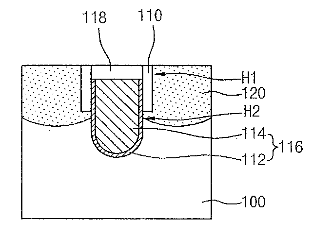
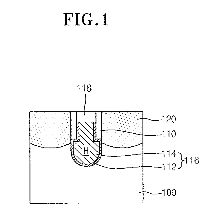
[0035]FIG. 1 is a sectional view illustrating a semiconductor device in accordance with the present invention. A groove H is defined in a semiconductor substrate 100, and a buried gate 116 is formed in the lower portion of the groove H such that the lower portion of the buried gate 116 is wider than the upper portion of the buried gate 116. The buried gate 116 preferably comprises a metal-based layer, for example, the buried gate 116 may include a titanium nitride layer 112 formed on the surfaces of the lower portion of the groove H. A barrier layer 110 and a tungsten layer 114 may be formed on the titanium nitride layer 112 to fill in the lower portion of the groove H. The barrier layer 110 is formed along the sidewalls of the upper portion of the buried gate 116 and along the sidewalls of the upper portion of the groove H. The barrier layer 110 preferably comprises, for example, a nitride layer at a thickness of preferably about 50˜500 Å. A capping layer 118 comprising an oxide la...

second embodiment

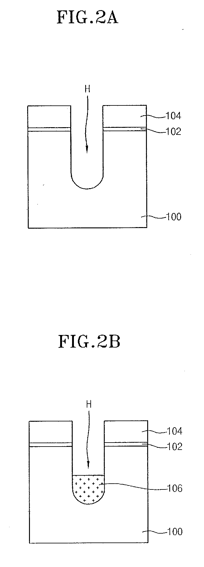
[0039]FIGS. 2A through 2H are sectional views illustrating the processes of a method for manufacturing a semiconductor device in accordance with the present invention.

[0040]Referring now to FIG. 2A, after sequentially forming a pad oxide layer 102 and a pad nitride layer 104 on a semiconductor substrate 100, by subsequently patterning the pad nitride layer 104 and the pad oxide layer 102, a gate forming region of the semiconductor substrate 100 is exposed. Then, by etching the exposed region of the semiconductor substrate 100, a groove H for a gate is defined within the semiconductor substrate 100.

[0041]Referring to FIG. 2B, after forming a sacrificial layer 106 to fill the groove H, the surface of the sacrificial layer 106 is subsequently planarized. The sacrificial layer 106 is preferably formed as a layer which is more easily etched than the barrier. That is, the sacrificial layer 106 has an etching selectivity with respect to a material layer for the barrier. Accordingly, the sa...

third embodiment

[0054]FIGS. 3A through 3D are sectional views illustrating the processes of a method for manufacturing a semiconductor device in accordance with the present invention.

[0055]Referring to FIG. 3A, similarly to the above-described second embodiment of the present invention, after defining a groove H by etching a semiconductor substrate 100, a barrier layer 110 is formed on the sidewalls of the upper portion of the groove H. Then, a buried gate 116 is formed to fill the lower portion of the groove H. The buried gate116 includes a gate insulation layer (not shown), a titanium nitride layer 112 and a tungsten layer 114 and the upper portion of the buried gate 116 is wider than the lower portion of the buried gate 116. Also shown are a pad oxide layer 102 and a pad nitride layer 104 on a semiconductor substrate 100.

[0056]Referring now to FIG. 3B, the barrier layer 110 is removed from the resultant semiconductor substrate 100 which is formed with the buried gate 116. At this time, when remo...


PUM


Abstract

A semiconductor device having a buried gate that can realize a reduction in gate-induced drain leakage is presented. The semiconductor device includes a semiconductor substrate, a buried gate, and a barrier layer. The semiconductor substrate has a groove. The buried gate is formed in a lower portion of the groove and has a lower portion wider than an upper portion. The barrier layer is formed on sidewalls of the upper portion of the buried gate.

Description

CROSS-REFERENCE TO RELATED APPLICATIONS[0001]The present application claims priority to Korean patent application number 10-2009-0049351 filed on Jun. 4, 2009, which is incorporated herein by reference in its entirety.BACKGROUND OF THE INVENTION[0002]The present invention relates to a semiconductor device and a method for manufacturing the same, and more particularly, to a semiconductor device which can realize a reduction in gate-induced drain leakage (GIDL) and a method for manufacturing the same.[0003]As the design rule for achieving more highly integrated semiconductor devices continues to demand decreases the critical dimensions, a problem can arise with regards to unwanted short channel effects across these resultant diminished channel lengths of the highly integrated transistors. Doping concentrations of a source region and a drain region may also need to be increased to enhance the electric fields which can also cause unwanted increases in junction leakage current. Due to th...

Claims


Application Information

Patent Timeline
Patent Type & Authority Applications(United States)
IPC IPC(8): H01L21/336
CPCH01L21/28238H01L29/4236H01L29/78H01L29/66621H01L29/66553H01L29/66348
Inventor YOO, MIN SOO
Owner SK HYNIX INC
Why Eureka
Try Eureka