Organic el device and method of manufacturing same

a technology of organic el and el glass, which is applied in the direction of thermoelectric devices, electroluminescent light sources, electric lighting sources, etc., can solve the problems of inability to apply film deposition methods developed as part of semiconductor processes to organic el devices, suffer marked degradation of light emission characteristics (current brightness characteristics), and achieve excellent light emission efficiency, and excellent moisture exclusion properties

Active Publication Date: 2011-11-17
SHARP KK
View PDF0 Cites 5 Cited by
  • Summary
  • Abstract
  • Description
  • Claims
  • Application Information

AI Technical Summary

Benefits of technology

[0020]In the circumstances of recent years in which there is a need to develop organic EL displays with higher light-emission efficiencies, this invention can provide an organic EL device which can maintain excellent light-emission efficiency over long periods by using a protective layer having excellent moisture exclusion properties. Further, because a protective layer of this invention has high visible-light transmissivity, a configuration of this invention is especially effective in top-emission organic EL devices.

Problems solved by technology

In addition to the realization of high-definition display, the attainment of long-term stability, including color reproducibility, is an important problem for the commercialization of organic EL displays as color display devices.
However, multicolor light-emitting organic EL displays have the drawback of suffering marked degradation of light emission characteristics (current-brightness characteristics) as a result of driving over a fixed period.
For this reason, film deposition methods which have been developed as part of semiconductor processes cannot be applied to organic EL devices, and there is the problem that a thin film for sealing, having adequate moisture exclusion properties, cannot be formed.
However, because the main bonds in silicon nitride films formed in the layered film are Si—N bonds, the change in lattice constants between the layers is small, defects in the layer serving as the substrate are carried over, and so there is the problem that silicon nitride film containing defects is formed.
In Japanese Patent Application Laid-open No. 2005-209356, the refractive index of the sealing film in the direction of light propagation is not stipulated, and so there is the drawback that transmissivity is low.
Further, when using a method in which the proportion of film deposition gas is changed continuously during the process of deposition of the protective film, because of the continuous growth of interfaces and other film defects formed due to differences in the film growth direction arising from misalignment of the atomic order, step formation and the like, such film defects may cause local declines in moisture exclusion properties.

Method used


Image

  • Organic el device and method of manufacturing same
  • Organic el device and method of manufacturing same
  • Organic el device and method of manufacturing same

Examples


embodiment 1

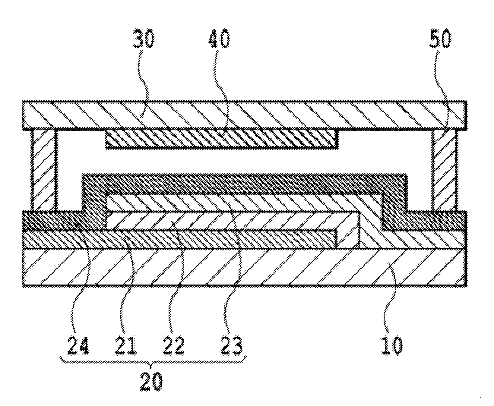
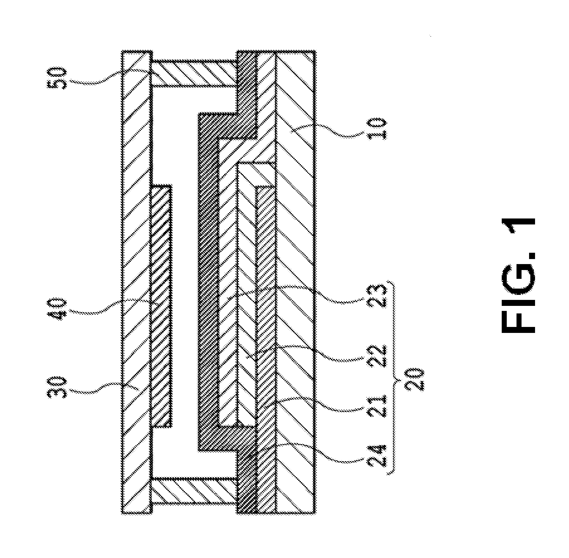
[0096]In this embodiment, a red light-emitting organic EL device with 2×2 pixels, with pixels measuring 0.3 mm×0.3 mm, was fabricated.

[0097]As the substrate 10, fusion glass (Corning 1737 glass, 50×50×1.1 mm) was prepared. A sputtering method was used to deposit an Ag film of thickness 100 nm on the substrate 10. The Ag film thus obtained was patterned using photolithography to form lower electrodes 21 comprising two stripe-shape electrodes, of width 0.3 mm.

[0098]Next, the substrate 10 with the lower electrodes 21 formed was installed in a resistive-heating evaporation deposition device. Through evaporation deposition using a mask, a buffer layer comprising Li of film thickness 1.5 nm was formed on the lower electrodes 21. Then, evaporation deposition was used to form an organic EL layer 22 comprising four layers, which were an electron transport layer / light-emitting layer / hole transport layer / hole injection layer. The electron transport layer was Alq3 with a film thickness of 20 nm...


PUM


Abstract

An organic EL device has an organic EL element provided on a substrate and includes a lower electrode, an organic EL layer, an upper electrode, and a protective layer for moisture protection, and a protective substrate laminated onto the organic EL element via an adhesive layer. The protective layer is a laminated body including first through nth layers, in order, from a side close to the upper electrode (where n is an integer equal to or greater than 3). Each layer of the protective layer includes silicon oxynitride or silicon nitride, and two adjacent layers layer have different chemical compositions. The first layer has a refractive index smaller than that of the upper electrode and the nth layer has a refractive index larger than that of the adhesive layer. The refractive index (k) of the kth layer satisfies a relationship: refractive index (k−1)>refractive index (k).

Description

BACKGROUND OF THE INVENTION[0001]1. Field of the Invention[0002]This invention relates to an organic EL device which is useful in display applications, and to a method of manufacturing such an organic EL device. More specifically, this invention relates to an organic EL device that prevents intrusion of water from the outside environment and exhibits excellent light emission efficiency over long periods of time, and to a method of manufacturing such an organic EL device.[0003]2. Description of the Related Art[0004]In display applications in recent years, there has been active research on organic EL devices employing light-emitting organic EL elements. Organic EL devices are expected to achieve high light emission brightness and light emission efficiency. This is because high current densities can be achieved at low voltages. In particular, high hopes are being placed in the display engineering field on high-definition multicolor light-emitting organic EL devices capable of multicolo...

Claims


Application Information

Patent Timeline
Patent Type & Authority Applications(United States)
IPC IPC(8): H01L51/52H01L51/56
CPCH01L51/5253H05B33/10H05B33/04H10K50/844H10K71/00
Inventor UTSUMI, MAKOTO
Owner SHARP KK
Why Eureka
Try Eureka