Polymer thin film, patterned media, production methods thereof, and surface modifying agents

a technology of patterned media and polymer thin film, which is applied in the direction of photomechanical equipment, instruments, transportation and packaging, etc., can solve the problems of large investment, large fabrication throughput, and large size devices, and achieve excellent regularity, reduced defects, and improved production efficiency

Inactive Publication Date: 2011-11-17
HITACHI LTD
View PDF1 Cites 24 Cited by
  • Summary
  • Abstract
  • Description
  • Claims
  • Application Information

AI Technical Summary

Benefits of technology

[0033]The present invention provides the polymer thin film having a finer structure than the conventional product, excellent regularity over a wide range and only limited defects on a substrate, patterned media, methods for producing the thin film and patterned media, and surface modifying agent used in these production methods.

Problems solved by technology

However, the top-down procedure needs larger-size devices and more sophisticated processes as the microstructures become finer to increase the production cost.
In particular, it needs vast investments when fabrication size of the microstructures decreases to an order of several tens of nanometers, because electron beams or deeply ultraviolet rays are needed for the patterning.
Moreover, fabrication throughput will greatly decrease, when formation of the microstructures with masks becomes difficult, because it needs the direct drawing procedure.

Method used


Image

  • Polymer thin film, patterned media, production methods thereof, and surface modifying agents
  • Polymer thin film, patterned media, production methods thereof, and surface modifying agents
  • Polymer thin film, patterned media, production methods thereof, and surface modifying agents

Examples


example 1

Measurement of Natural Period d0 of Block Copolymer

[0140]Example 1 first prepared the block copolymer for forming the polymer thin film.

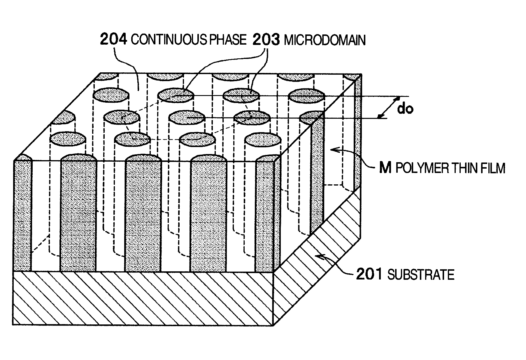
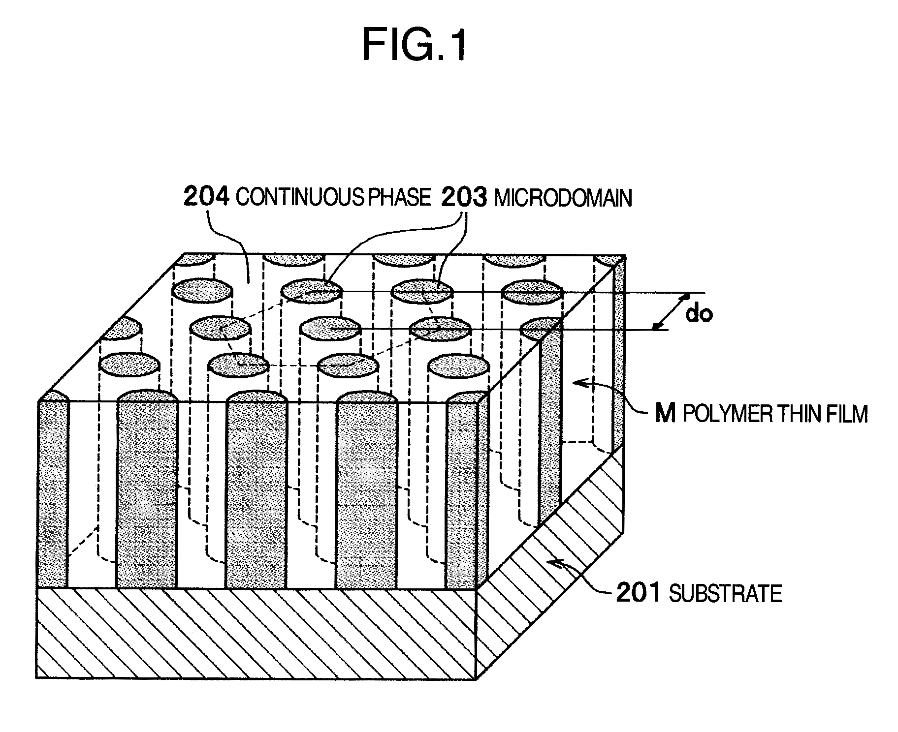
[0141]More specifically, the copolymer of polymethylmethacrylate-block-poly3-(3,5,7,9,11,13,15-heptaisobutyl-pentacyclo[9.5.|3,9.|5,15|7,13]octacyloxan-1-yl)propylmethacrylate (PMMA-b-PMAPOSS) was prepared, wherein the PMMA segment corresponding to the second segment A2 (refer to FIG. 6) had a number-average molecular weight Mn of 4,100, and PMAPOSS segment corresponding to the first segment A1 (refer to FIG. 6) had a number-average molecular weight Mn of 26,900.

[0142]The copolymer was referred to as the “first” block copolymer “PMMA(4.1 k)-b-PMAPOSS (26.9 k),” as shown in Table 1. The first block copolymer had a polydisperse index Mw / Mn of the overall molecular weight distribution of 1.03, by which was meant that the copolymer was microphase-separated into the columnar microdomains 203 of PMMA and continuous phase of the PMAPOSS.

TABLE 1Number-avera...

example 2

[0174]Example 2 also used the block copolymer of polymethylmethacrylate-block-poly3-(3,5,7,9,11,13,15-heptaisobutyl-pentacyclo[9.5.|3,9.|5,15|7,13]octacyloxan-1-yl)propylmethacrylate (PMMA-b-PMAPOSS), wherein the PMMA segment corresponding to the second segment A2 (refer to FIG. 6) had a number-average molecular weight Mn of 4,900, and PMAPOSS segment corresponding to the first segment A1 (refer to FIG. 6) had a number-average molecular weight Mn of 32,500.

[0175]The block copolymer was referred to as the “second” block copolymer PMMA(4.9 k)-b-PMAPOSS (32.5 k) as shown in Table 1. The second block copolymer had a polydisperse index Mw / Mn of the overall molecular weight distribution of 1.03, by which was meant that the copolymer was microphase-separated into the columnar microdomains 203 of PMMA and continuous phase of the PMAPOSS.

[0176]The second block copolymer was measured for its natural period d0 in the same manner as in Example 1. It was 30 nm.

[0177]This example patterned, as wi...

example 3

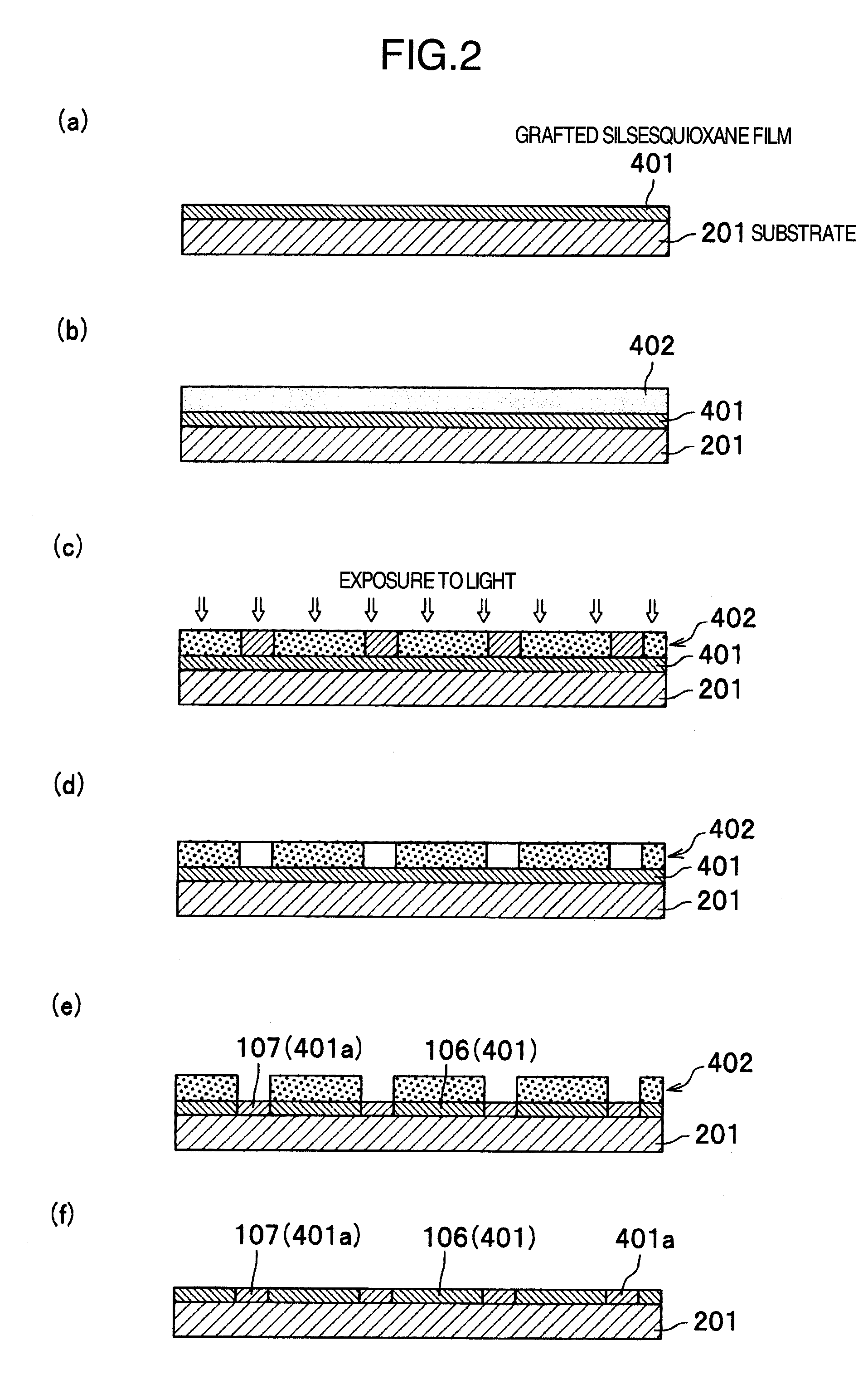
[0201]Example 3 describes an embodiment of producing a pattern substrate (patterned media). This example decomposed the columnar microdomains and removed them from the polymer thin film M following the steps shown in FIGS. 7 (a) and (b), in order to form the porous thin film on the substrate.

[0202]Example 3 produced the microphase-separated structure with the columnar microdomains 203 of PMMA upstanding on the substrate 201 (extending in the polymer thin film M thickness direction) following the procedure adopted in Example 1 (refer to FIG. 7 (a)). This example also adopted the pattern shown in FIG. 9, as in Example 1. The second block copolymer was also used, as in Example 1.

[0203]Next, PMMA-b-PMAPOSS was spread on the substrate 201 chemically patterned at intervals of 48 nm, which was twice as long as natural period d0 (24 nm) of PMMA-b-PMAPOSS, to have the 40 nm thick film. The film was then exposed to the vapor of carbon disulfide solvent to develop the microphase-separated stru...


PUM

PropertyMeasurementUnit
lattice-lattice distanceaaaaaaaaaa
chemical propertiesaaaaaaaaaa
thicknessaaaaaaaaaa

Abstract

The objects of the present invention are to provide a polymer thin film having finer structure than the conventional product, excellent regularity over a wide range and only limited defects, patterned media, methods for producing the thin film and patterned media, and surface modifying agent used in these production methods.
The method of the present invention is for producing a polymer thin film with a plurality of microdomains regularly arranged in a continuous phase by microphase separation on a substrate, comprising steps for forming a grafted silsesquioxane film on the substrate, and for forming a pattern different in chemical properties from the grafted silsesquioxane film in such a way that the pattern corresponds to the microdomain arrangement.

Description

TECHNICAL FIELD[0001]The present invention relates to a polymer thin film having a microstructure formed by microphase separation of a block copolymer on a substrate, patterned media using the polymer thin film, methods for producing the thin film and patterned media, and surface modifying agent used in these production methods.BACKGROUND OF THE INVENTION[0002]Recently, demands have been increasing for fine, regularly arranged patterns having a size of several nanometers to several hundreds of nanometers formed on substrates to satisfy the requirements for compacter, more functional electronic devices, energy-storage devices, sensors and so on. Therefore, demands have been also increasing for establishing processes which can produce fine, regularly arranged patterns (hereinafter simply referred to as the “microstructures”) at high accuracy and low cost.[0003]The top-down procedures represented by lithography have been generally adopted for producing these microstructures, in which a...

Claims


Application Information

Patent Timeline
Patent Type & Authority Applications(United States)
IPC IPC(8): B32B3/10C08L83/00B05D5/00
CPCG03F7/0752G03F7/11G03F7/16Y10T428/24802C08F297/026C08G77/045C08F220/14C08F2230/085
Inventor TADA, YASUHIKOYOSHIDA, HIROSHIHAYAKAWA, TERUAKIHIRAI, TOMOYASUISHIDA, YOSHIHITO
Owner HITACHI LTD
Why Eureka
Try Eureka