Photovoltaic cell

a photovoltaic cell and photovoltaic technology, applied in the direction of photovoltaic energy generation, basic electric elements, electrical equipment, etc., can solve the problems of poor material quality, difficult to accurately control the thickness of the n-doped layer, and much lower efficiency solar cells as photo-generated charge carriers recombine more readily within the device. achieve the effect of better thermal transfer characteristics

Inactive Publication Date: 2011-12-15
IQE SILICON COMPOUNDS
View PDF3 Cites 18 Cited by
  • Summary
  • Abstract
  • Description
  • Claims
  • Application Information

AI Technical Summary

Benefits of technology

[0014]The processing of Ge wafers to form a diffused lower junction for solar cells tends to be restricted to maximum 100 mm wafer sizes, and the use of a GaAs wafer substrate widens access to larger wafer sizes such as 150 mm and 200 mm which are more widely available in GaAs.
[0015]Typically, the one or more first layers will have been grown epitaxially on or over a GaAs substrate, so as to provide optimal GaAs lattice matching, but in an operable device the GaAs substrate may have been removed as discussed below, for example taking advantage of the etch-stop effect of the Ge or SiGe layer when etching GaAs. To this end, the one or more first layers may be grown directly on and contacting a GaAs surface provided by the substrate. Havin...

Problems solved by technology

Mismatches in lattice spacing of more than a small fraction of 1% lead to growth defects which result in poor material quality and a much lower efficiency solar cell as photo-generated charge carriers recombine more readily within the device.
However, using the descr...

Method used


Image

  • Photovoltaic cell
  • Photovoltaic cell
  • Photovoltaic cell

Examples


Embodiment Construction

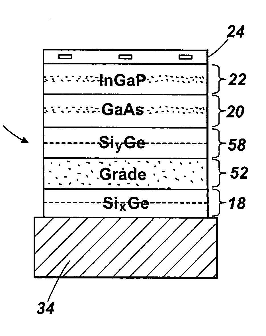
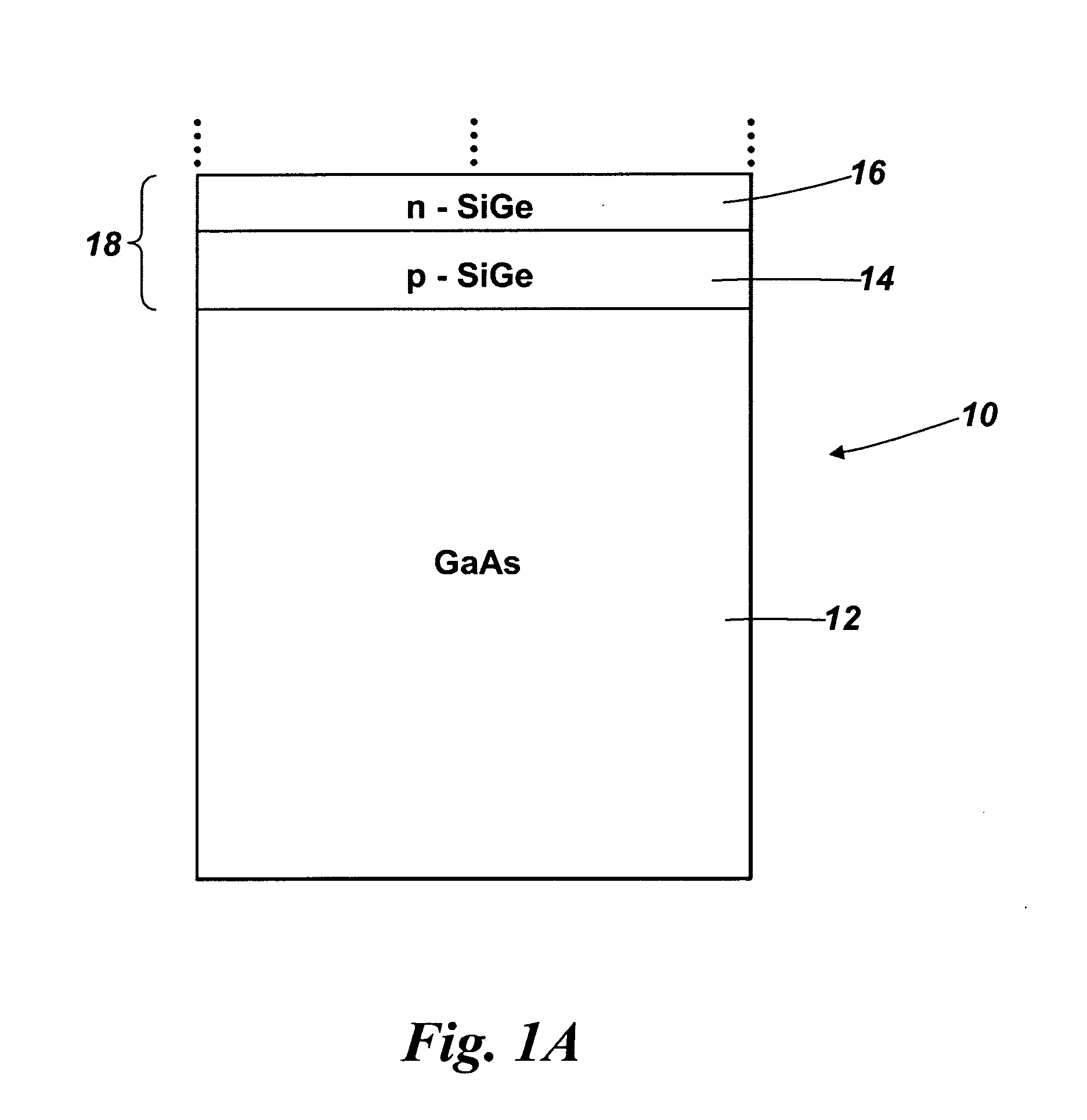
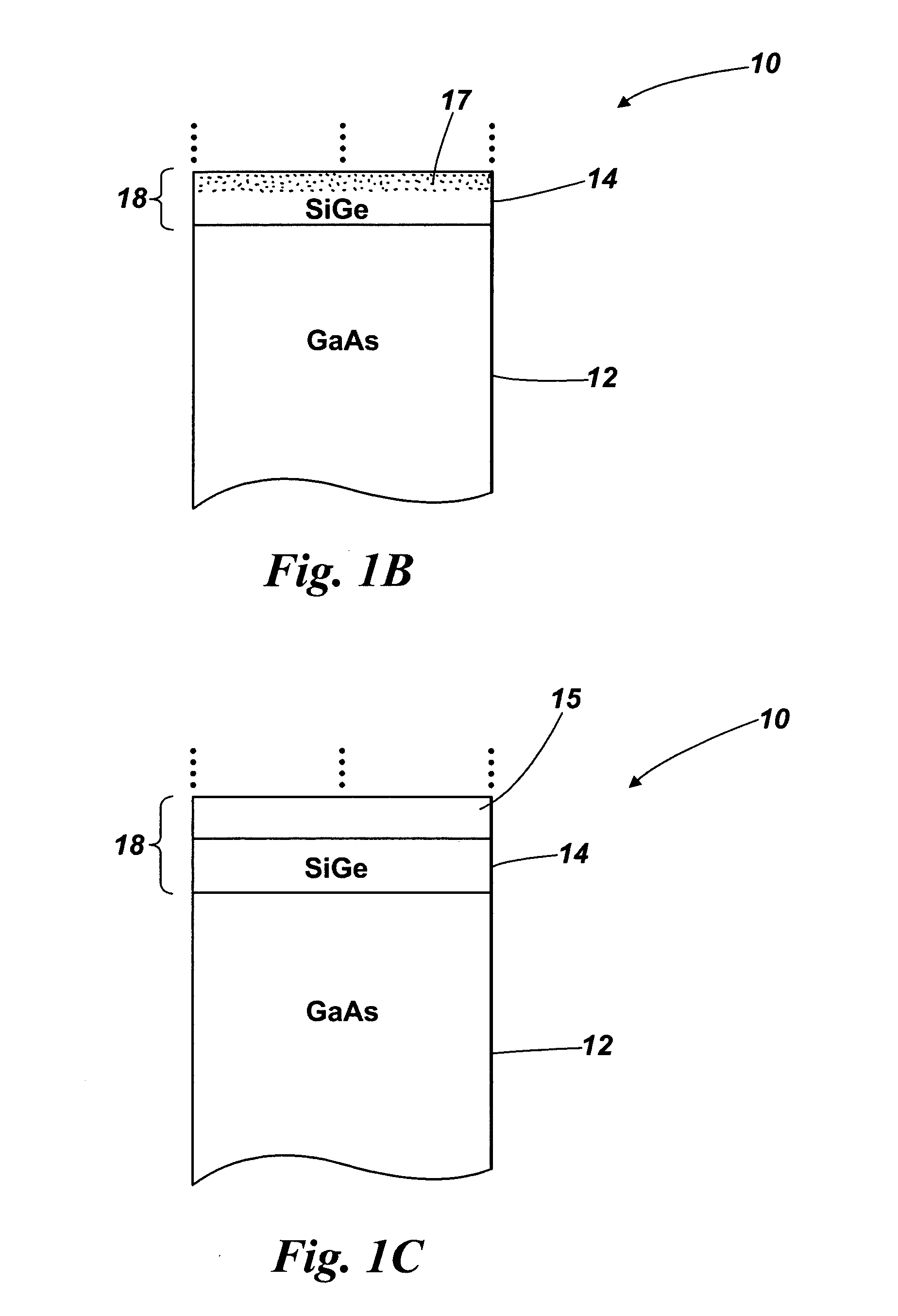
[0033]Referring to FIG. 1A there is shown schematically a photovoltaic cell structure 10 according to a first embodiment of the invention. The structure 10 comprises a GaAs substrate 12. On the GaAs substrate are two successive first layers 14, 16 of a SiGe material grown epitaxially on and monolithically with the GaAs substrate, and these layers together form a first germanium based photovoltaic junction 18. The first layers of SiGe have a silicon content selected so as to be substantially lattice matched to the GaAs substrate. To achieve this the silicon fraction x for SixGe1-x could lie in the range of 0˜0.04, more preferably 0.01˜0.03 and more preferably still about 0.016˜0.02. To form a practical photovoltaic junction the lower SiGe layer may typically be p-doped to a concentration of about 5×10¹⁶ to 5×1019 cm−3 and have a thickness of about 1˜2 μm. The upper SiGe layer may typically be n-doped to a concentration of about 1×1017 cm−3 and have a thickness of about 0.2˜1 μm.

[0034...


PUM


Abstract

There is disclosed a photovoltaic cell, such as a solar cell, incorporating one or more epitaxially grown layers of SiGe or another germanium material, substantially lattice matched to GaAs. A GaAs substrate used for growing the layers may be removed by a method which includes using a boundary between said GaAs and the germanium material as an etch stop.

Description

FIELD OF THE INVENTION[0001]The present invention relates to photovoltaic cells, and in particular, but not exclusively, to multi-junction solar cells in which a lower photovoltaic junction for absorbing longer wavelength parts of the solar spectrum is germanium based.INTRODUCTION[0002]Photovoltaic cells convert light energy, for example sunlight, into useful electrical power. Typically, electron-hole pairs are formed by absorption of photons in a semiconductor material close to a p-n junction which acts to separate the charge carriers which are then delivered to an electric circuit through metallic contacts on the cell device. The absorption process only occurs if a photon has an energy higher than a bandgap of the local semiconductor material, so that a lower bandgap material tends to absorb more photons. Excess energy of a particular photon over the bandgap energy is lost as heat into the semiconductor lattice. If the p-n junction is formed of materials with a higher bandgap, low...

Claims


Application Information

Patent Timeline
IPC IPC(8): H01L31/109H01L31/18H01L31/0312H01L31/0687
CPCH01L31/028Y02E10/544H01L31/18H01L31/0687Y02E10/547H01L31/042H01L31/068H01L31/1808H01L31/1812H01L31/0682H01L31/0684
Inventor HARPER, ROBERT CAMERON
Owner IQE SILICON COMPOUNDS
Why Eureka
Try Eureka