Photoelectric conversion device and method for manufacturing the same

Inactive Publication Date: 2011-12-22
SEMICON ENERGY LAB CO LTD
View PDF8 Cites 9 Cited by
  • Summary
  • Abstract
  • Description
  • Claims
  • Application Information

AI Technical Summary

Benefits of technology

[0029]Note that in this specification, an “intrinsic semiconductor” refers to not only a so-called intrinsic semiconductor in which the Fermi level lies in the middle of the band gap, but a semiconductor in which the concentration of an impurity imparting p-type or n-type conductivity is 1×1020 cm−3 or lower and photoconductivity is 100 times or more as high as the dark conductivity. This intrinsic semiconductor may include an impurity element belonging to Group 13 or Group 15 of the periodic table. Accordingly

Problems solved by technology

In any case, the method in which the silicon substrate itself is etched to form the uneven structure on the surface of the silicon substrate is not favorable because the method has a problem in controllability of the uneven shape and affects the characteristics of the solar c

Method used


Image

  • Photoelectric conversion device and method for manufacturing the same
  • Photoelectric conversion device and method for manufacturing the same
  • Photoelectric conversion device and method for manufacturing the same

Examples


Example

Embodiment 1

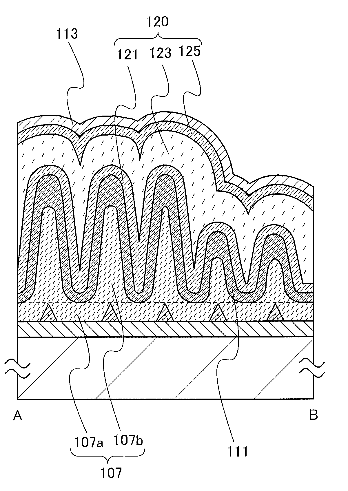
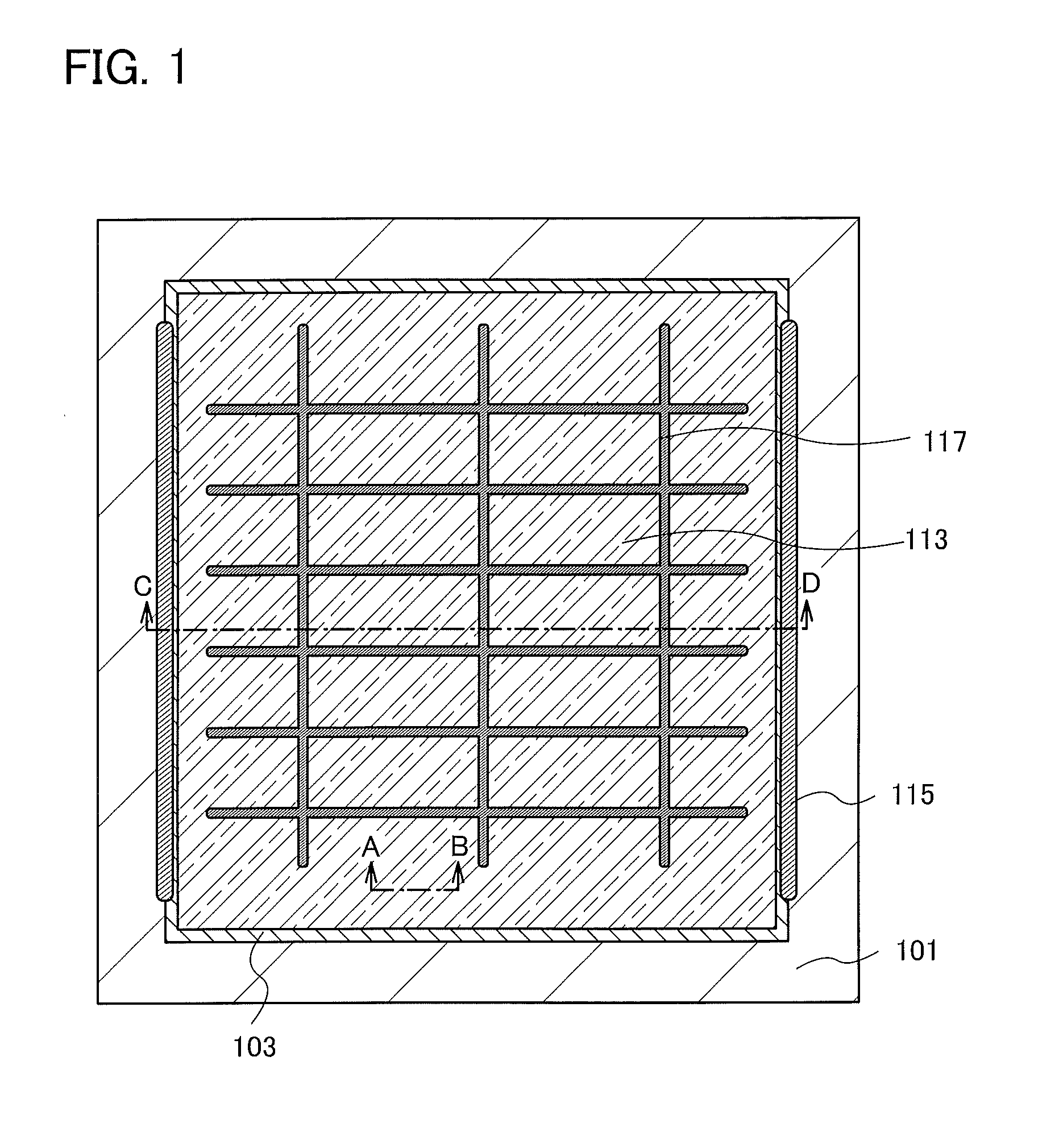
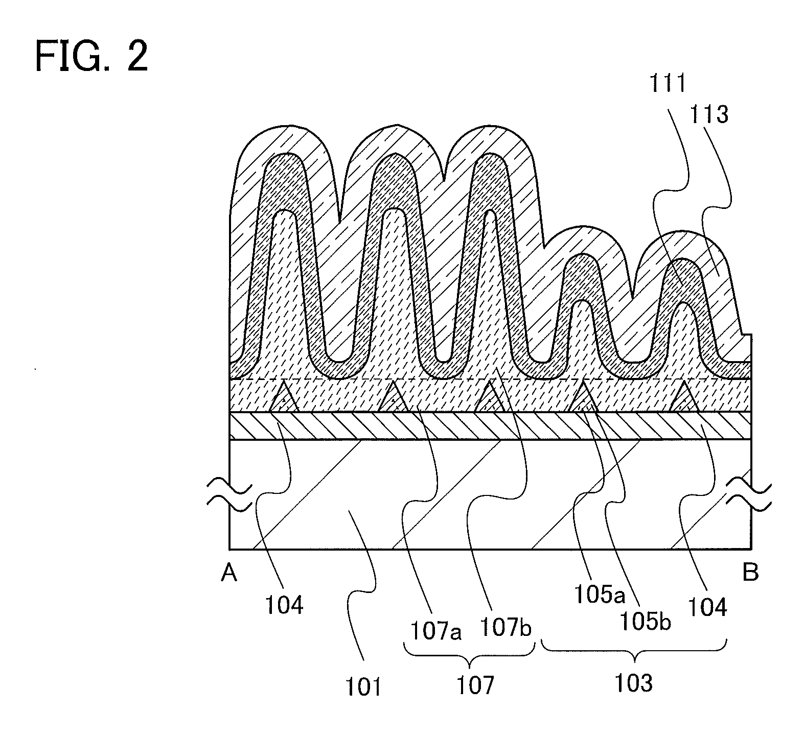
[0044]In this embodiment, a structure of a photoelectric conversion device which is one embodiment of the present invention is described with reference to FIG. 1, FIG. 2, FIG. 3, FIG. 4, and FIGS. 5A to 5C.

[0045]FIG. 1 is a schematic view of a top surface of a photoelectric conversion device. Although not illustrated, a photoelectric conversion layer is formed over an electrode 103 which is formed over a substrate 101. Further, an auxiliary electrode 115 is formed over the electrode 103 and a grid electrode 117 is formed over a second-conductivity-type crystalline semiconductor region. The auxiliary electrode 115 functions as a terminal for extracting electric energy to the outside. The grid electrode 117 is formed over the second-conductivity-type crystalline semiconductor region to reduce resistance of the second-conductivity-type crystalline semiconductor region. Here, a cross section of a dashed-and-dotted line A-B in FIG. 1 is described with reference to FIG. 2, FIG...

Example

Embodiment 2

[0096]In this embodiment, a photoelectric conversion device in which the size of a second conductive layer and the size of a mixed layer are different as compared to those in Embodiment 1 is described with reference to FIG. 7 and FIG. 8.

[0097]The cross section of the dashed-and-dotted line A-B in FIG. 1 is described with reference to FIG. 7 and FIG. 8.

[0098]FIG. 7 is a schematic view of a photoelectric conversion device including the substrate 101, the electrode 103, a first-conductivity-type crystalline semiconductor region 110, and a second-conductivity-type crystalline semiconductor region 112. The second conductivity type is opposite to the first conductivity type. The first-conductivity-type crystalline semiconductor region 110 and the second-conductivity-type crystalline semiconductor region 112 function as a photoelectric conversion layer.

[0099]In this embodiment, the electrode 103 includes the first conductive layer 104, a plurality of second conductive layers 15...

Example

Embodiment 3

[0111]In this embodiment, a method for manufacturing a photoelectric conversion layer which has fewer defects than the photoelectric conversion layer in Embodiment 1 is described.

[0112]After one or more of the first-conductivity-type crystalline semiconductor region 107, the first-conductivity-type crystalline semiconductor region 108, the first-conductivity-type crystalline semiconductor region 110, the crystalline semiconductor region 109, the second-conductivity-type crystalline semiconductor region 111, and the second-conductivity-type crystalline semiconductor region 112, which are described in Embodiments 1 and 2, are formed, the temperature of a reaction chamber in an LPCVD apparatus is set at a temperature of higher than or equal to 400° C. and lower than or equal to 450° C., introduction of a source gas into the LPCVD apparatus is stopped, and hydrogen is introduced. Then, in a hydrogen atmosphere, heat treatment at a temperature of higher than or equal to 400° ...


PUM

PropertyMeasurementUnit
Temperatureaaaaaaaaaa
Lengthaaaaaaaaaa
Lengthaaaaaaaaaa

Abstract

An object of the present invention is to provide a photoelectric conversion device having a novel anti-reflection structure. An uneven structure is formed on a surface of a semiconductor by growth of the same or a different kind of semiconductor instead of forming an anti-reflection structure by etching a surface of a semiconductor substrate or a semiconductor film. For example, a semiconductor layer including a plurality of projections is provided on a light incident plane side of a photoelectric conversion device, thereby considerably reducing surface reflection. Such a structure can be formed by a vapor deposition method; therefore, the contamination of the semiconductor is not caused.

Description

BACKGROUND OF THE INVENTION[0001]1. Field of the Invention[0002]The present invention relates to a photoelectric conversion device and a method for manufacturing the same.[0003]2. Description of the Related Art[0004]Recently, a photoelectric conversion device, which is a power generation means that generates power without carbon dioxide emissions, has attracted attention as a countermeasure against global warming. A solar cell for supplying residential power or the like, which generates power from sunlight outdoors, is known as a typical example thereof. For such a solar cell, a crystalline silicon solar cell using single crystal silicon or polycrystalline silicon is mainly used.[0005]An uneven structure is provided on a surface of a solar cell using a single crystal silicon substrate or a polycrystalline silicon substrate in order to reduce surface reflection. The uneven structure provided on the surface of the silicon substrate is formed by etching the silicon substrate with an al...

Claims


Application Information

Patent Timeline
IPC IPC(8): H01L31/06H01L31/18C23C16/24H01L31/0224H01L31/0236H01L31/068H01L31/075H01L31/078
CPCH01L31/0236H01L31/028H01L31/035281Y02E10/547H01L31/075Y02E10/548H01L31/068Y02E10/546H01L31/022425H01L31/03529H01L31/078H01L31/182Y02P70/50H01L31/06H01L31/04H01L31/18
Inventor KATAISHI, RIHOKURIKI, KAZUTAKA
Owner SEMICON ENERGY LAB CO LTD
Why Eureka
Try Eureka