Semiconductor device and method of manufacturing the same

a technology of semiconductor devices and semiconductors, applied in semiconductor devices, semiconductor/solid-state device details, electrical apparatus, etc., can solve problems such as problems, and the inability to prevent the island b>101/b> from being lifted up

Active Publication Date: 2011-12-29
SEMICON COMPONENTS IND LLC
View PDF7 Cites 8 Cited by
  • Summary
  • Abstract
  • Description
  • Claims
  • Application Information

AI Technical Summary

Benefits of technology

[0017]The invention also provides a method of manufacturing a semiconductor device. The method includes providing a lead frame having an island and a first lead. The first lead is separated from the island so that, in plan view of the lead frame, an edge of the first lead faces an edge of the island. The lead frame also has a first protrusion protruding, in the plan view, from the edge of the island toward an extrapolation of the edge of the first lead. The method further includes holding down the first protrusion of the island using a damper, attaching a first end of a metal ribbon to an electrode of a semiconductor element disposed on the island of the lead frame while the first protrusion is being held down by the damper, and attaching a second end of the metal ribbon to the first lead.

Problems solved by technology

When the island 101 is lifted up, some problems occur.
Furthermore, even if the holes could be formed there, the suction force is insufficient because the area drawn by suction is too small, and it is accordingly impossible to prevent the island 101 from being lifted up.

Method used


Image

  • Semiconductor device and method of manufacturing the same
  • Semiconductor device and method of manufacturing the same
  • Semiconductor device and method of manufacturing the same

Examples


Embodiment Construction

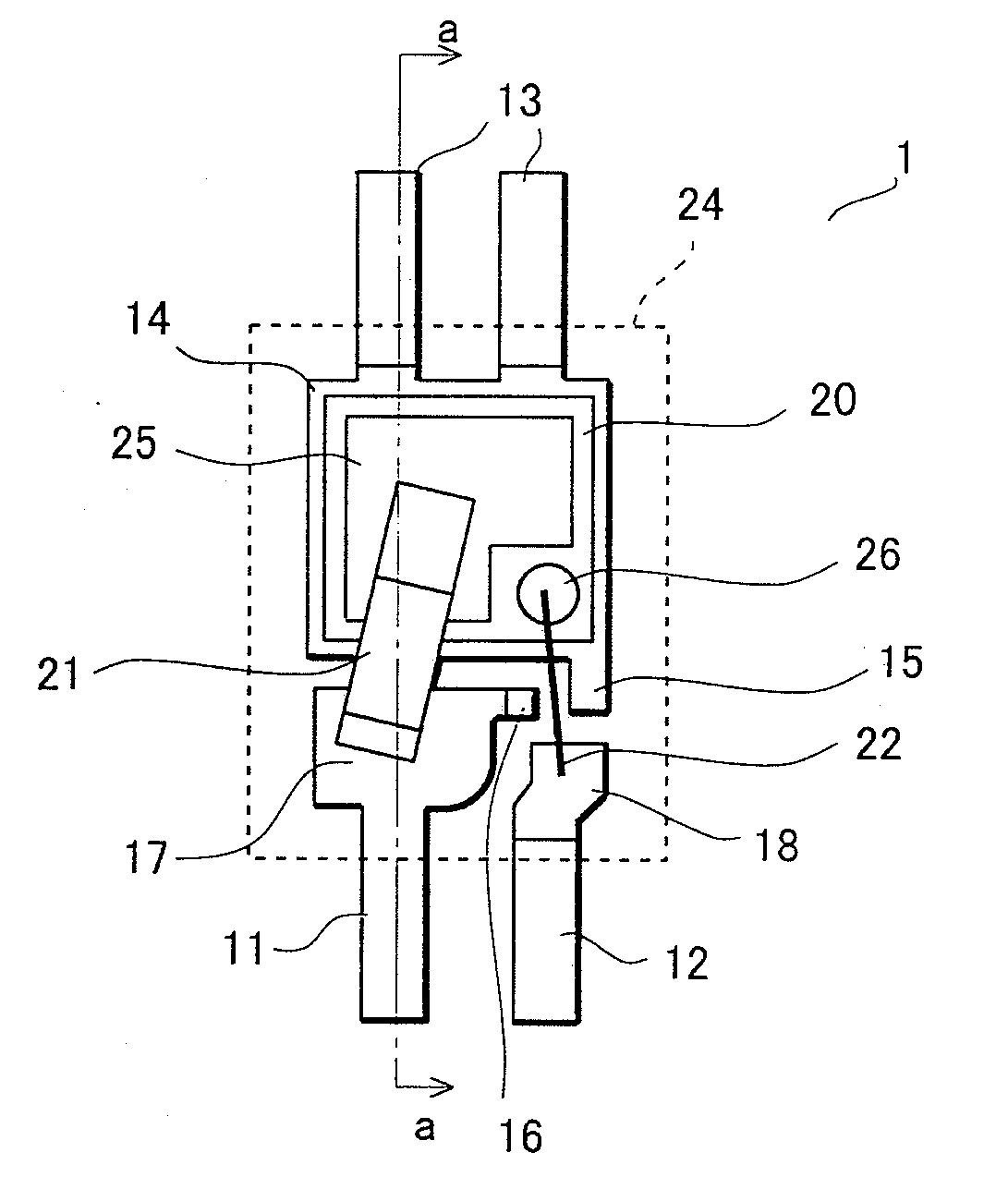
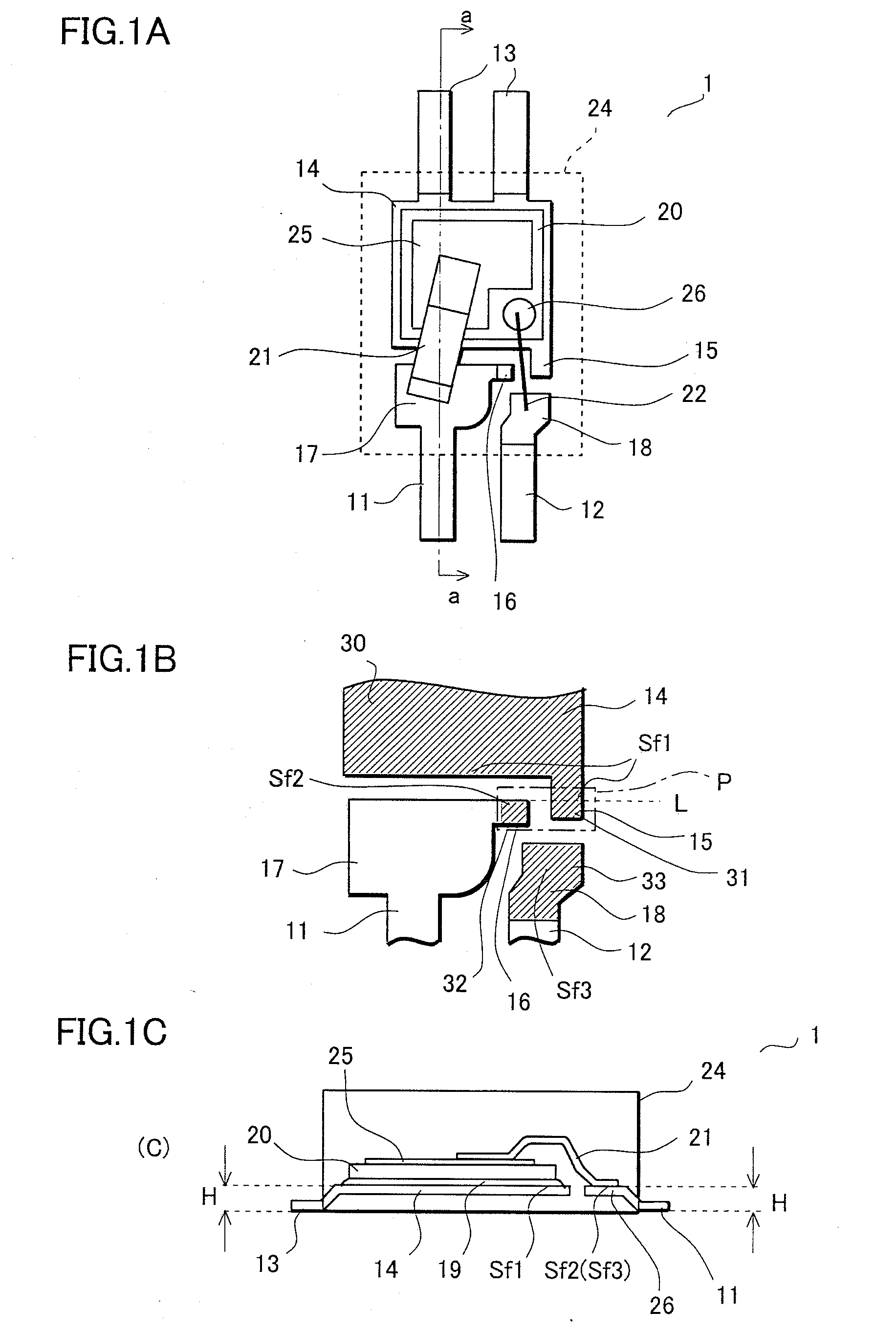
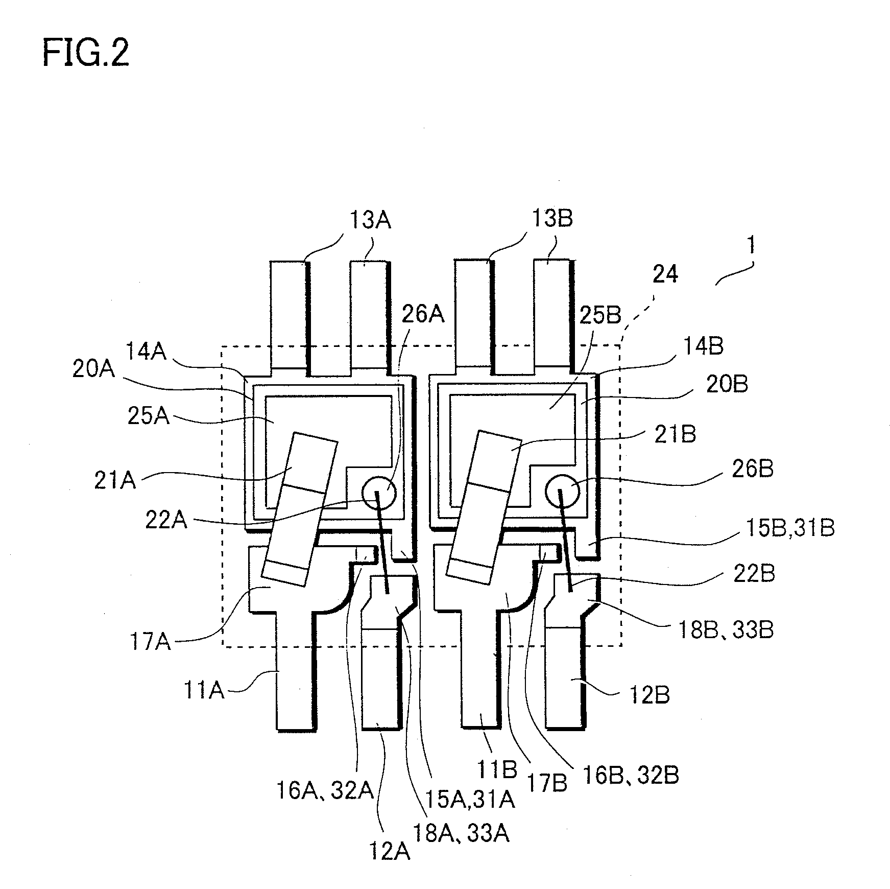
[0027]Detailed descriptions will be provided for the embodiments of the present invention while referring to FIGS. 1A to 8. FIGS. 1A, 1B and 1C are views showing a semiconductor device 1 of a first embodiment. FIG. 1A is a plan view of the semiconductor device 1; FIG. 1B is a main-part enlarged view of FIG. 1A; and FIG. 1C is a cross-sectional view taken along the line a-a of FIG. 1A.

[0028]Referring to FIG. 1A, the semiconductor device 1 includes a semiconductor element 20, an island 14, a first lead 11, a second lead 12, third leads 13, a protrusion 15, a metal ribbon 21 and a sealing resin 24.

[0029]A MOSFET (Metal-Oxide Semiconductor Field Effect Transistor), a bipolar transistor, an IGBT (Insulated Gate Bipolar Transistor), an IC (Integrated Circuit), a diode, or something similar may be used for the semiconductor element 20. Hereunder, the embodiments of the present invention will be clarified by giving an example in which an MOSFET is used for the semiconductor element 20. A so...


PUM


Abstract

When a metal ribbon is ultrasonic-bonded, a peripheral area of an island and hanging pins provided in the periphery of the island need to be clamped by use of clampers of a bonder to prevent the island from being lifted up. However, if no sufficiently-wide peripheral area of the island can be secured or no hinging pins can be provided due to the miniaturization of the device, there arises a problem that the island cannot be clamped. A protrusion, which protrudes toward a lead and has the same height as an end portion of the lead, is provided to an edge of the island opposed to the lead. Accordingly, when the protrusion and the end portion of the lead are simultaneously pressed by the damper, it is possible to prevent the island from being lifted up even when no hanging pin or no clamp area around the island is provided.

Description

[0001]This application claims priority from Japanese Patent Application Number JP 2010-148092 filed on Jun. 29, 2010, the content of which is incorporated herein by reference in its entirety.BACKGROUND OF THE INVENTION[0002]1. Field of the Invention[0003]The present invention relates to a semiconductor device and a method of manufacturing the same. Particularly, the present invention relates to: a semiconductor device including a metal ribbon for connecting an electrode of a semiconductor element and a lead together; and a method of manufacturing the same.[0004]2. Description of the Related Art[0005]Descriptions will be provided for a conventional semiconductor device 100 while referring to FIGS. 9A and 9B. FIG. 9A is a plan view of the semiconductor device 100, and FIG. 9B is a plan view showing a part of a manufacturing process.[0006]Referring to FIG. 9A, the conventional semiconductor device 100 includes: an island 101; a semiconductor element 103 fixedly bonded to the top surfac...

Claims


Application Information

Patent Timeline
Patent Type & Authority Applications(United States)
IPC IPC(8): H01L23/495H01L21/58
CPCH01L21/565H01L23/3107H01L23/49524H01L23/49562H01L23/49575H01L24/34H01L24/73H01L24/97H01L2224/48247H01L2224/48465H01L2224/73219H01L2224/73221H01L2224/73263H01L2224/73265H01L2224/97H01L2924/01013H01L2924/01029H01L2924/01046H01L2924/01047H01L2924/01078H01L2924/01079H01L2924/01082H01L24/48H01L2224/32245H01L2924/01005H01L2924/01006H01L2924/01033H01L2924/014H01L2924/13091H01L2924/12041H01L2924/13055H01L2224/84205H01L24/29H01L24/32H01L24/83H01L24/84H01L24/85H01L24/92H01L2224/04034H01L2224/04042H01L2224/06181H01L2224/291H01L2224/29139H01L2224/2919H01L2224/37124H01L2224/45144H01L2224/83439H01L2224/83464H01L2224/85439H01L2224/85464H01L2224/92246H01L2924/1305H01L2924/14H01L2224/40247H01L2224/84464H01L2224/92157H01L2924/15747H01L2924/07802H01L2924/1306H01L2224/83H01L2224/84H01L2224/85H01L2924/00H01L2924/00012H01L2224/45015H01L2224/48639H01L2224/48664H01L2924/181H01L2224/40095H01L24/40H01L2224/40245H01L24/37H01L2924/00014H01L24/45H01L2224/45014H01L2224/83801H01L2224/84214H01L2224/05552H01L2224/05554H01L2224/0603H01L2224/8385H01L2924/207H01L2924/206
Inventor URUSHIHATA, HIROYOSHI
Owner SEMICON COMPONENTS IND LLC
Why Eureka
Try Eureka