System and method for extending vco output voltage swing

a technology of output voltage and swing, applied in the field of voltage control of oscillators, can solve the problems of increasing chip cost, increasing phase noise, and limited output voltage swing, and achieve the effect of increasing output voltage swing and increasing output voltage swing

Inactive Publication Date: 2012-01-05
QUINTIC MICROELECTRONICS WUXI
View PDF8 Cites 26 Cited by
  • Summary
  • Abstract
  • Description
  • Claims
  • Application Information

AI Technical Summary

Benefits of technology

[0006]A method for increasing the output voltage swing is disclosed for a VCO system having LC resonant circuit. The method includes providing DC-blocked cross coupling from the drains of the transistor pair to the gates of the transistor pair. The method also includes providing an offset voltage to the gates of the transistor pair to reduce the maximum gate-to-drain voltage for the NMOS transistor pair or the maximum drain-to-gate voltage for the PMOS transistors so that the transistor pair will work in the saturation region.

Problems solved by technology

The direct cross coupling of the MOS transistor pair will result in limited output voltage swing since a large swing may cause the MOS transistors into a linear region to increase phase noise.
Nevertheless, this method needs an additional inductor, which will increase chip cost noticeably if the additional inductor is integrated on chip.
Furthermore, for a wide band LC VCO, the LC noise filter resonant frequency is difficult to change with VCO frequency.

Method used


Image

  • System and method for extending vco output voltage swing
  • System and method for extending vco output voltage swing
  • System and method for extending vco output voltage swing

Examples


Embodiment Construction

[0015]In radio frequency (RF) systems, the local oscillator (LO) phase noise degrades the received SNR by a process known as reciprocal mixing. Voltage controlled oscillator (VCO) having LC resonant circuit is often used to generate the desired LO frequency. Such VCO determines the LO high frequency, i.e., the higher end of the PLL loop band width, phase noise. The phase noise of the VCO having an LC resonant circuit is usually characterized by Leeson's proportionality, published D. B. Leeson, entitled “A Simple Model of Feedback Oscillator Noise Spectrum,” in Proceedings IEEE, Vol. 54, pp. 329-330, February 1966:

L(wm)∝1V2·kTC·w0Q·1wm2,(1)

where V is the VCO output-voltage swing. In the above equation, phase noise is proportional to the thermal noise kT / C and is shaped in frequency by the LC tank and normalized to the power in the oscillation amplitude. Furthermore, w0 is the center frequency, wm is an offset frequency, and Q is the Q value of the LC circuit.

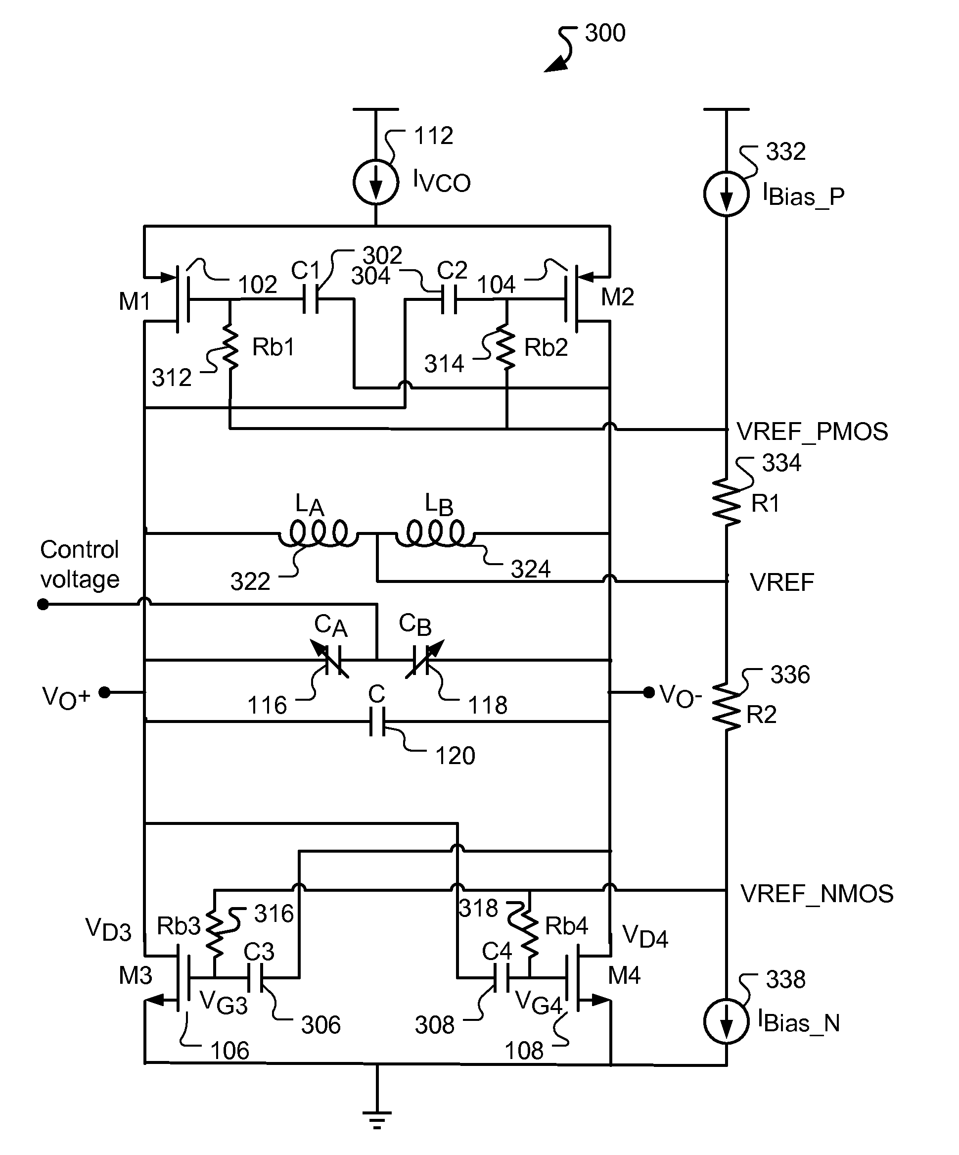
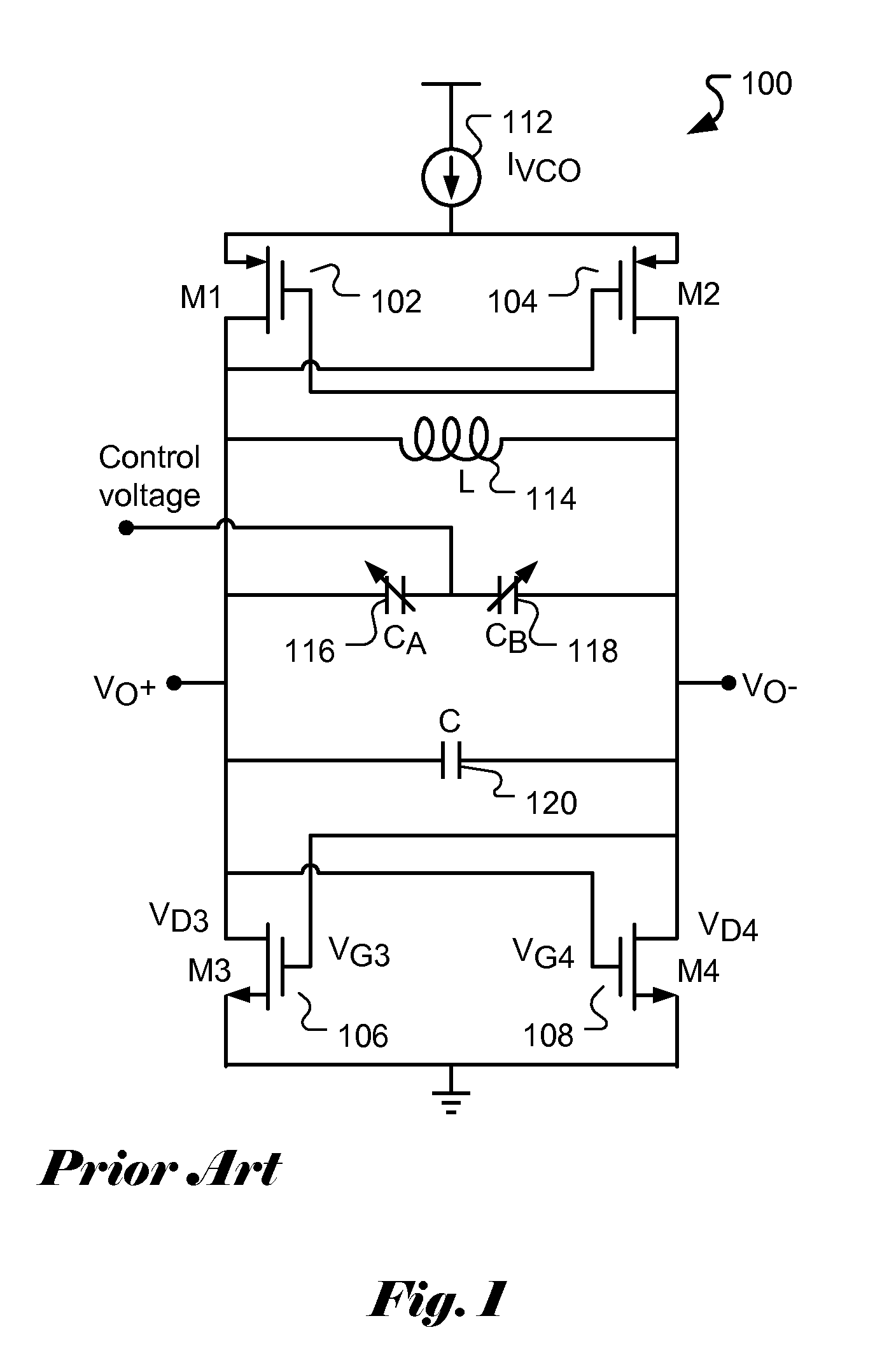
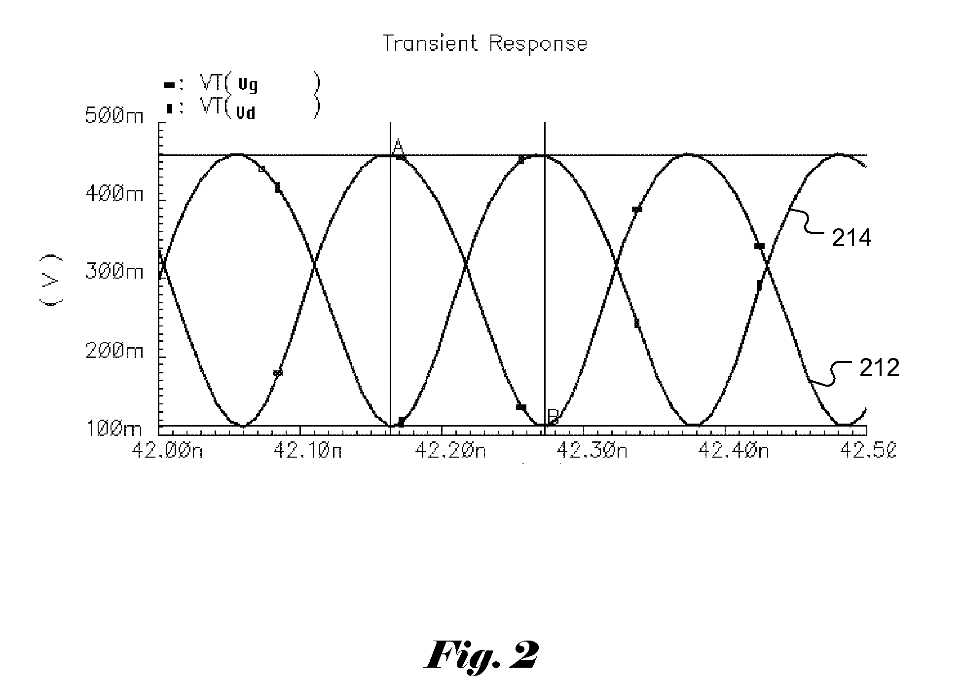
[0016]FIG. 1 illustrates ...


PUM


Abstract

Voltage controlled oscillator (VCO) has been widely used in radio frequency communication systems. In a typical VCO implementation, a pair of directly cross-coupled MOS transistors is used as a switching device and an LC resonant circuit is used to tune the desired frequency. The direct cross coupling of the MOS transistor pair will result in limited output voltage swing since a large swing may cause the MOS transistors into a linear region to increase phase noise. The VCO system to increase the output voltage swing according to one embodiment of the present invention includes DC-blocking capacitors to avoid direct cross coupling of the MOS pair. The VCO further includes circuit to provide bias for the gate voltage of the MOS pair. A method for increasing the output voltage swing is disclosed for a VCO system having LC resonant circuit. The method includes providing DC-blocked cross coupling from the drains of the cross-coupled transistor pair to the gates of the cross-coupled transistor pair. The method also includes providing an offset voltage to the gates of the cross-coupled transistor pair to reduce the maximum gate-to-drain voltage of a cross-coupled NMOS transistor pair or maximum drain-to-gate voltage of a cross-coupled PMOS transistor pair so that the cross-coupled transistor pair will work in a saturation region when the output voltage swing is increased.

Description

CROSS REFERENCE TO RELATED APPLICATIONS[0001]The present invention claims priority to U.S. Provisional Patent Application, No. 61 / 360,501, filed Jul. 1, 2010, entitled “System and Method for Extending VCO Output Voltage Swing.” The U.S. Provisional Patent Application is hereby incorporated by reference in its entirety.FIELD OF THE INVENTION[0002]The present invention relates to voltage controlled oscillator. In particular, the present invention relates to extending the output voltage swing of a VCO having LC resonant circuit.BACKGROUND[0003]Voltage controlled oscillator has been widely used in radio frequency communication systems. In a typical VCO implementation, a pair of directly cross-coupled MOS transistors is used as a switching device and an LC resonant circuit is used to tune the desired frequency. The direct cross coupling of the MOS transistor pair will result in limited output voltage swing since a large swing may cause the MOS transistors into a linear region to increase...

Claims


Application Information

Patent Timeline
Patent Type & Authority Applications(United States)
IPC IPC(8): H03B5/12
CPCH03B5/1228H03B5/1243H03B5/1212
Inventor YANG, YULI, XUECHULIU, RONGXUAN, PEIQI
Owner QUINTIC MICROELECTRONICS WUXI
Why Eureka
Try Eureka