Soi mos device having bts structure and manufacturing method thereof

a technology of soi mos and manufacturing method, which is applied in the direction of semiconductor devices, basic electric elements, electrical apparatus, etc., can solve the problems of complex manufacturing process, high cost of thin silicon film, and difficult control of the threshold voltage of fully depleted soi mos, so as to improve the bts structure, eliminate floating body effects, and eliminate floating body effects

Inactive Publication Date: 2012-01-19
SHANGHAI INST OF MICROSYSTEM & INFORMATION TECH CHINESE ACAD OF SCI
View PDF2 Cites 6 Cited by
  • Summary
  • Abstract
  • Description
  • Claims
  • Application Information

AI Technical Summary

Benefits of technology

[0025]A SOI MOS device having BTS structure and manufacturing method thereof is provided in the present invention. The advantages of the present invention are listed as below. The SOI MOS device has improved BTS structure, and there are two divided heavily doped N-type regions in the source region, a heavily doped P-type region formed between these two heavily doped N-type regions and a silicide formed on the mentioned heavily doped N-type regions and heavily doped P-type region. There is an ohmic contact, which is formed between the heavily doped P-type region and the silicide thereon, could release the holes accumulated in body region of the SOI MOS device and eliminate floating body effects thereof. Besides, these two heavily doped N-type region which are covered by the silicide could effectively eliminate floating body effects without increasing the chip area and also overcome the disadvantages such as decreased effective channel width of the devices in the BTS structure of the prior art. Furthermore, the devices in the present invention could be fabricated via simplified fabricating process with great compatibility with traditional CMOS technology.

Problems solved by technology

In one hand, the thin silicon film has high cost, and in the other hand, the threshold voltage of the fully depleted SOI MOS is hard to control.
However, there are still some disadvantages such as complex manufacturing process, increased parasitic effect, degraded electric properties and increased device area.
However, the BTS structure in the prior art always results in the asymmetry of the MOS devices and decreased effective channel width of the devices.

Method used


Image

  • Soi mos device having bts structure and manufacturing method thereof
  • Soi mos device having bts structure and manufacturing method thereof
  • Soi mos device having bts structure and manufacturing method thereof

Examples


first embodiment

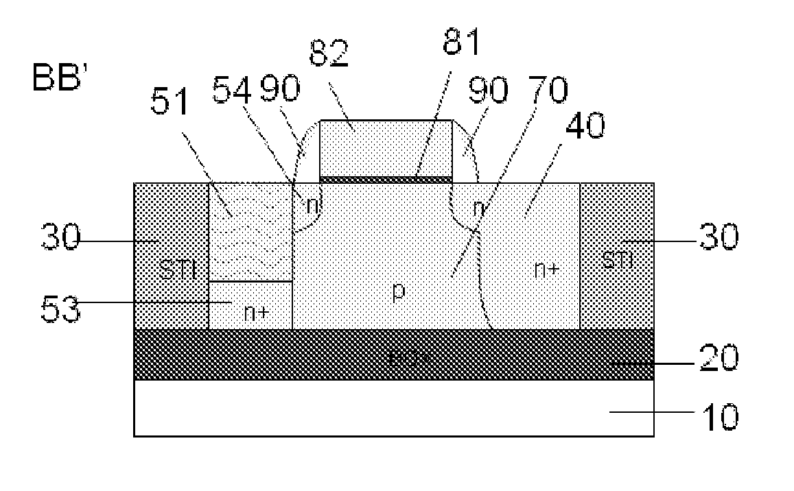
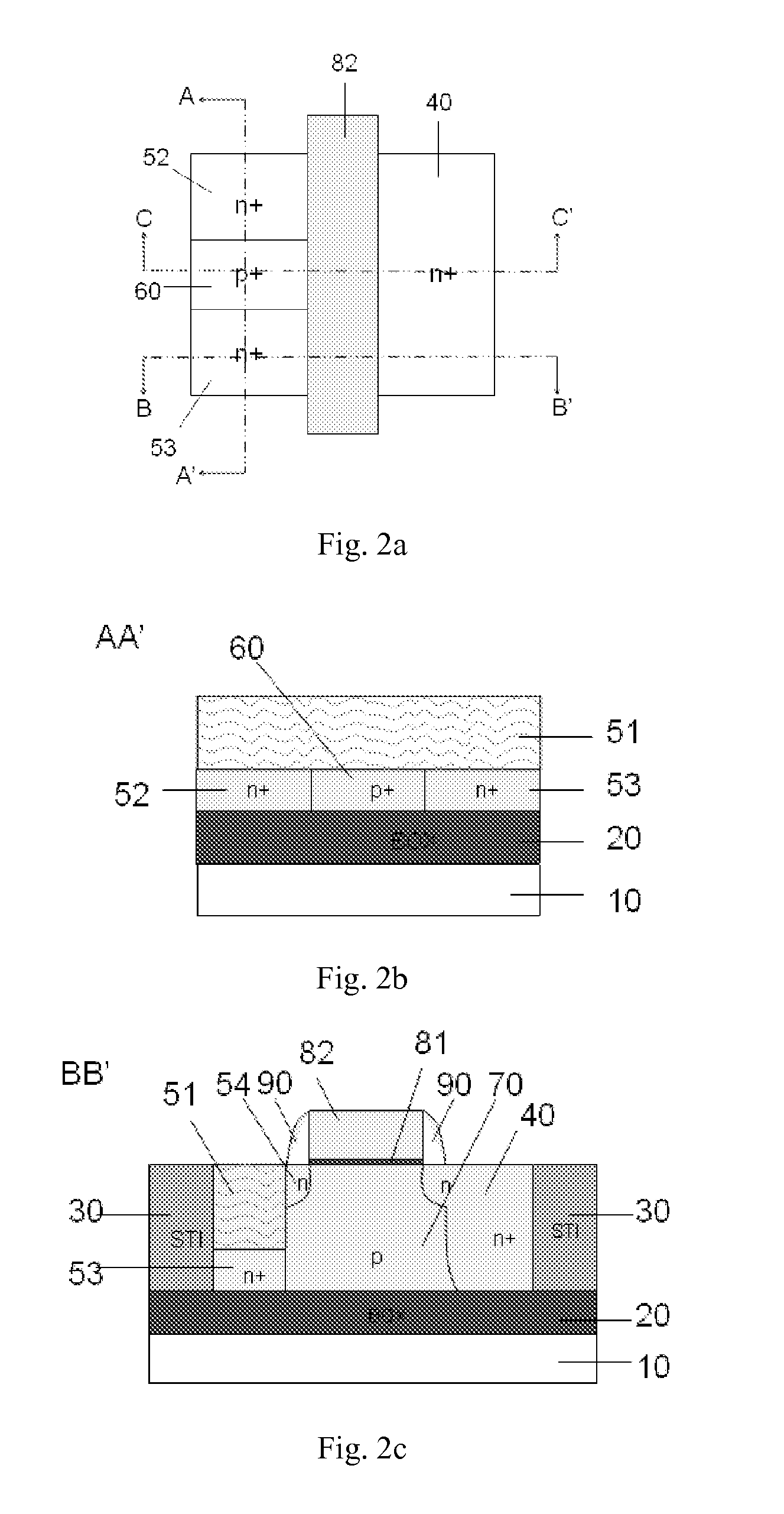
[0031]FIG. 2a-2d show the systematic structure of a SOI MOS device having BTS structure, and the SOI MOS device includes: a semiconductor substrate 10, a buried oxide layer (BOX) 20 formed on the semiconductor substrate 10; an active region formed on the buried oxide layer 20 and a shallow trench isolation (STI) region 30 formed surrounding the active region.

[0032]The active region includes a gate region, a body region 70 formed under the gate region, an N-type source region and an N-type drain region 40 which are located on the two opposite ends of the body region 70, and the N-type source region and the N-type drain region 40 are located on the opposite side of the gate region.

[0033]The N-type source region includes: two heavily doped N-type regions 52 and 53, a heavily doped P-type region 60, a silicide 51 and a shallow N-type region 54. The heavily doped P-type region 60 is formed between the heavily doped N-type region 52 and the heavily doped N-type region 53. The silicide 51 ...


PUM


Abstract

The present invention discloses a SOI MOS device having BTS structure and manufacturing method thereof. The source region of the SOI MOS device comprises: two heavily doped N-type regions, a heavily doped P-type region formed between the two heavily doped N-type regions, a silicide formed above the heavily doped N-type regions and the heavily doped P-type region, and a shallow N-type region which is contact to the silicide; an ohmic contact is formed between the heavily doped P-type region and the silicide thereon to release the holes accumulated in body region of the SOI MOS device and eliminate floating body effects thereof without increasing the chip area and also overcome the disadvantages such as decreased effective channel width of the devices in the BTS structure of the prior art. The manufacturing method comprises steps of: forming a heavily doped P-type region via ion implantation, forming a metal layer above the source region and forming a silicide via the heat treatment between the metal layer and the Si underneath. The device in the present invention could be fabricated via simplified fabricating process with great compatibility with traditional CMOS technology.

Description

FIELD OF THE INVENTION [0001]The present invention relates to a manufacturing method of a MOS (Metal Oxide Semiconductor) structure, more particularly to a SOI MOS device having BTS structure and manufacturing method thereof, which belongs to semiconductor manufacturing field.BACKGROUND OF THE INVENTION[0002]SOI means silicon on insulator. In SOI technique, devices usually are fabricated in a thin silicon film and a buried oxide layer (BOX) is disposed between the device and the substrate to separate them. Comparing to traditional bulk silicon, SOI technology has many advantages, such as reduced parasitic capacitance making SOI device provide higher speed and consume less power, full dielectric isolation of the SOI CMOS device eliminating the occurrence of bulk-Si CMOS device parasitic latch-up effects and making SOI technique have superior performances including high integration density, and good anti-irradiation properties. SOI technique has been widely applied in many technical f...

Claims


Application Information

Patent Timeline
Patent Type & Authority Applications(United States)
IPC IPC(8): H01L29/78H01L21/336
CPCH01L29/458H01L29/78621H01L29/78615
Inventor CHEN, JINGLUO, JIEXINWU, QINGQINGHUANG, XIAOLUWANG, XI
Owner SHANGHAI INST OF MICROSYSTEM & INFORMATION TECH CHINESE ACAD OF SCI
Why Eureka
Try Eureka