Substrate processing apparatus, substrate processing method and non-transitory computer storage medium

a substrate processing and processing method technology, applied in semiconductor/solid-state device testing/measurement, television systems, instruments, etc., can solve the problems of inability to use the above-described transfer apparatus for another wafer, inability to make the work distance between the image capture apparatus and the illumination apparatus (half mirror) longer, and inability to appropriately perform the inspection of the wafer in some cases. , to achieve the effect of improving the throughput of substrate processing

Active Publication Date: 2012-01-19
TOKYO ELECTRON LTD
View PDF1 Cites 15 Cited by
  • Summary
  • Abstract
  • Description
  • Claims
  • Application Information

AI Technical Summary

Benefits of technology

[0016]According to the present invention, it is possible to obtain, in inspection of a substrate after edge exposure processing, a precise image with no distortion of image and appropriately perform inspection while improving the throughput of substrate processing including the inspection.

Problems solved by technology

However, in the inspection apparatus described in Japanese Patent Application Laid-open No. 2007-240519, the arrangement of the image capturing apparatus, the illumination apparatus and the half mirror in plan view is determined because there is restriction on the apparatus space, and therefore it is difficult to make the work distance between the image capturing apparatus and the illumination apparatus (half mirror) longer.
Therefore, a distortion may occur in the image of the wafer captured by the image capturing apparatus, so that the inspection of the wafer cannot be appropriately performed in some cases.
In this case, during the transfer of the wafer from the edge exposure apparatus to the inspection apparatus, it is impossible to use the above-described transfer apparatus for another wafer.
In other words, the other wafer sometimes needs to be kept waiting even though the other wafer has undergone processing and is able to be transferred to another processing apparatus, resulting in occurrence of waiting for transfer.

Method used


Image

  • Substrate processing apparatus, substrate processing method and non-transitory computer storage medium
  • Substrate processing apparatus, substrate processing method and non-transitory computer storage medium
  • Substrate processing apparatus, substrate processing method and non-transitory computer storage medium

Examples


Embodiment Construction

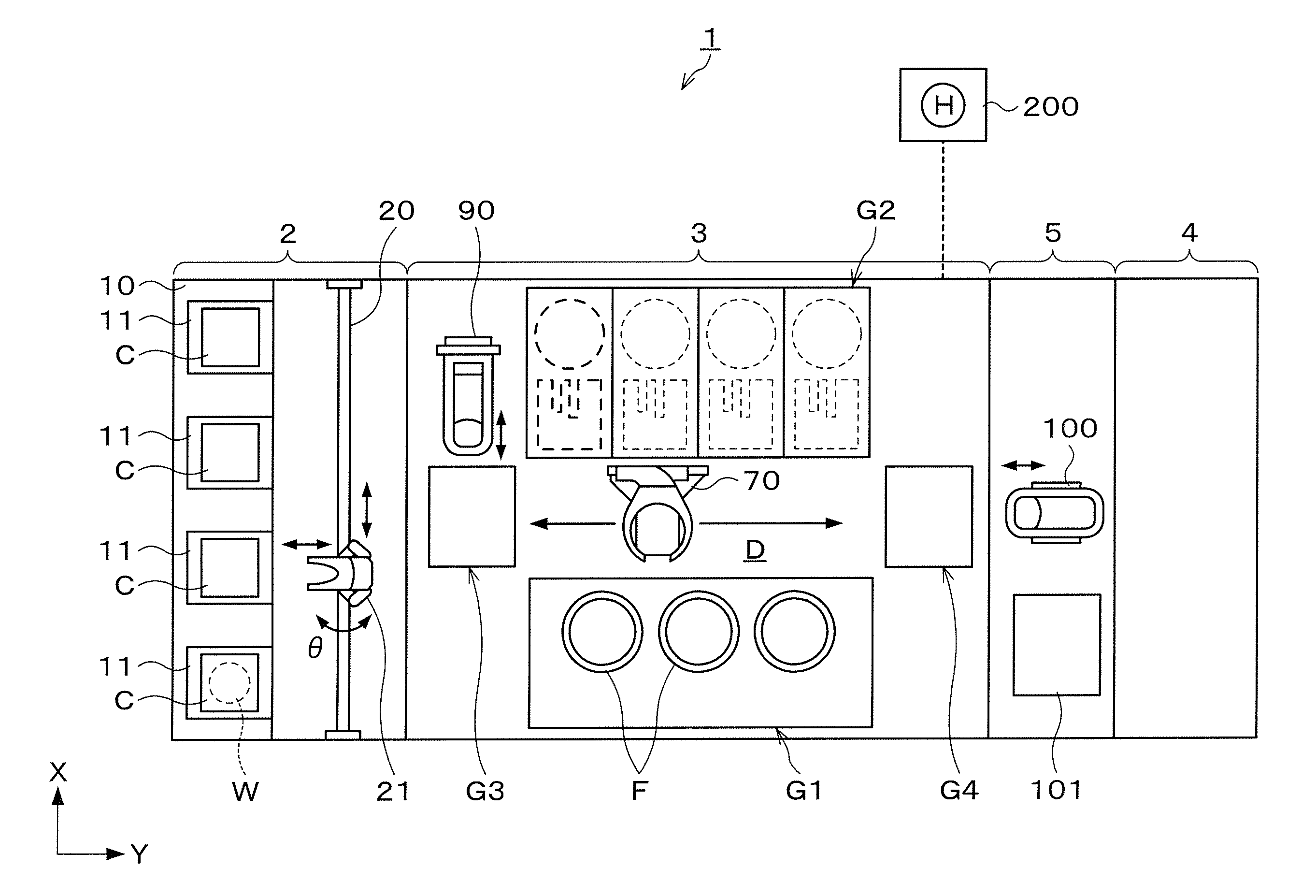
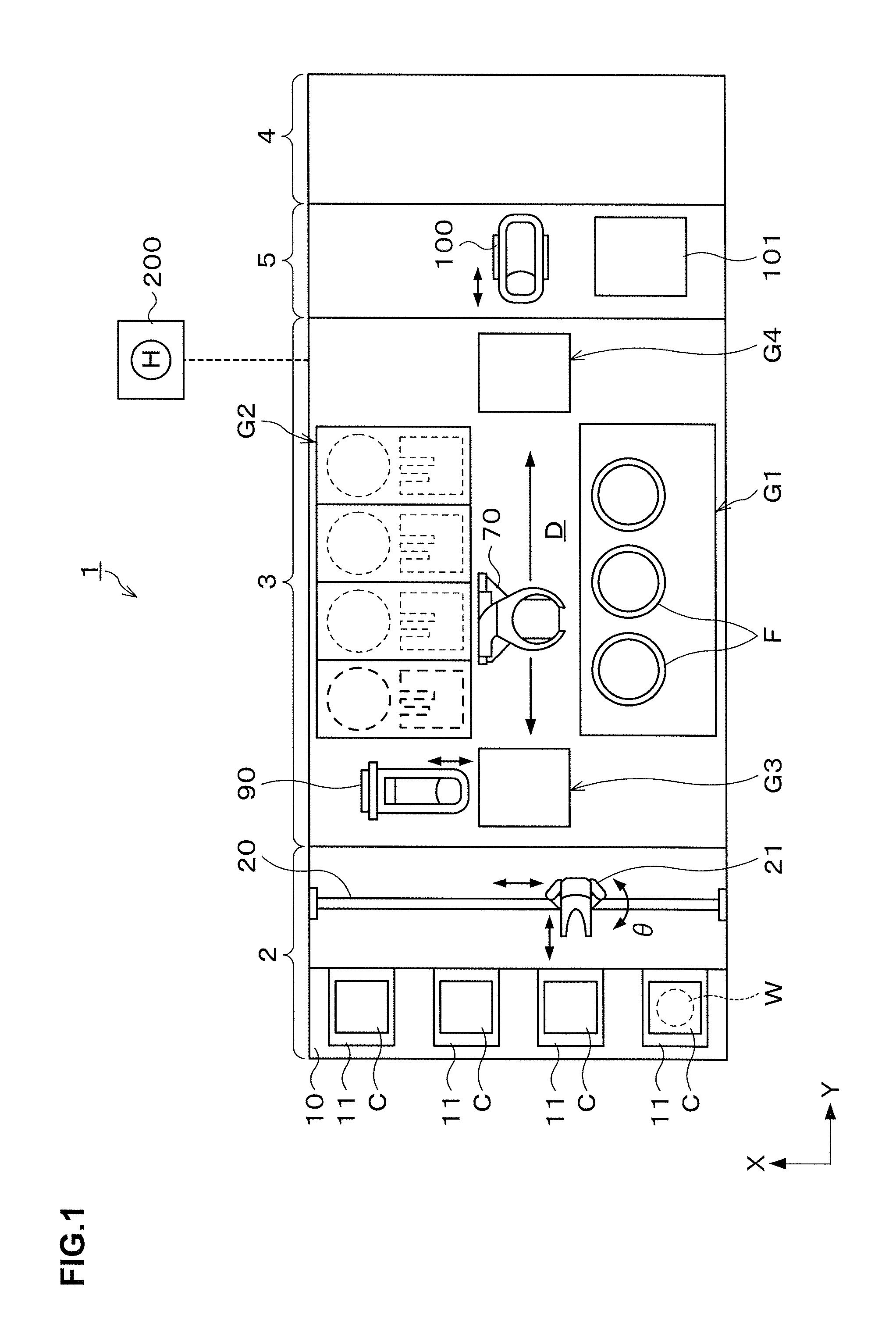
[0029]Hereinafter, embodiments of the present invention will be described. FIG. 1 is a plan view showing the outline of the internal configuration of a coating and developing treatment system including a wafer processing apparatus as a substrate processing apparatus according to this embodiment. FIG. 2 and FIG. 3 are side views showing the outline of the internal configuration of the coating and developing treatment system 1.

[0030]The coating and developing treatment system 1 has, as shown in FIG. 1, a configuration in which, for example, a cassette station 2 to / from which a cassette C housing a plurality of wafers W therein is transferred from / to the outside, a processing station 3 including a plurality of various kinds of processing and treatment apparatuses for performing predetermined processing or treatment in a manner of single wafer processing in the photolithography processing, and an interface station 5 for delivering the wafers W to / from an aligner 4 adjacent to the proces...


PUM


Abstract

A substrate processing apparatus includes: a holding unit holding a substrate; a rotation driving unit rotating the substrate held on the holding unit; a moving mechanism moving the holding unit between a delivery position and an edge exposure position; an exposure unit provided on the edge exposure position side and exposing an edge portion of a coating film above the substrate held on the holding unit; an image capturing unit provided on the edge exposure position side and above the exposure unit and capturing an image of the substrate held on the holding unit; and a direction change unit changing a direction of an optical path formed between the substrate held on the holding unit and the image capturing unit. The direction change unit includes a first reflecting mirror, a second reflecting mirror, and a third reflecting mirror.

Description

BACKGROUND OF THE INVENTION[0001]1. Field of the Invention[0002]The present invention relates to a substrate processing apparatus, a substrate processing method and a non-transitory computer storage medium.[0003]2. Description of the Related Art[0004]In a photolithography processing in manufacture of a semiconductor device, for example, resist coating treatment of applying a resist solution onto a semiconductor wafer (hereinafter, referred to as a “wafer”) to form a resist film, edge exposure processing of selectively exposing an edge portion of the resist film, exposure processing of exposing the resist film whose edge portion has been exposed to a predetermined pattern, developing treatment of developing the exposed resist film and so on are performed in sequence to form a predetermined resist pattern on the wafer.[0005]Further, the wafer which is subjected to the photolithography processing as described above is subjected to so-called macro defect inspection by an inspection appa...

Claims


Application Information

Patent Timeline
Patent Type & Authority Applications(United States)
IPC IPC(8): H04N7/18
CPCH01L21/67288H01L21/6715G01B11/303G01B11/306G01N2021/9563G01N2021/95638G03F1/60H01L21/0274H01L22/10H01L22/24
Inventor KOGA, NORIHISA
Owner TOKYO ELECTRON LTD
Why Eureka
Try Eureka