Semiconductor drive device

Active Publication Date: 2012-02-02
FUJI ELECTRIC CO LTD
View PDF2 Cites 3 Cited by
  • Summary
  • Abstract
  • Description
  • Claims
  • Application Information

AI Technical Summary

Benefits of technology

[0009]As a result of this, semiconductor device fuses and fuses that cut off the drive circuit power source are unnecessary, and it is possible to reduce the size of the device, and to reduce the part replacement time at a time of failure recovery.
[0010]Furthermore, as an operation of the me

Problems solved by technology

However, with this method, a fuse is also necessary in the circuit through which the main current flows in order to detect a failure of the semiconductor device, meaning that in a large capacity device, t

Method used


Image

  • Semiconductor drive device
  • Semiconductor drive device
  • Semiconductor drive device

Examples


Example

Example 1

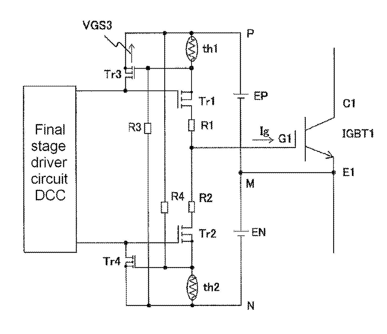
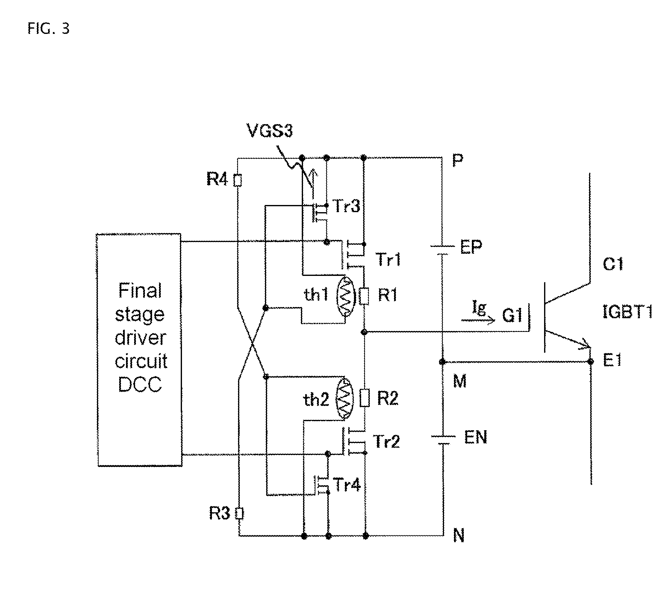
[0025]FIG. 3 shows a first example of the invention. The difference from FIG. 1, which is a heretofore known circuit, is that thermistors (in this example, PTC thermistors whose resistance values increase in accordance with a temperature rise) th1 and th2 whose resistance values change depending on the temperature are installed in gate resistors R1 and R2, the drain and source of a P-channel type MOSFET Tr3 are connected between the gate and source of a P-channel type MOSFET Tr1, which is a forward biasing switching element, the drain and source of an N-channel type MOSFET Tr4 are connected between the gate and source of an N-channel type MOSFET Tr2, which is a reverse biasing switching element, a series circuit of the thermistor th1 and resistor R3 and a series circuit of the thermistor th2 and resistor R4 are connected between the positive electrode of a forward biasing power source EP and the negative electrode of a reverse biasing power source, the gate of the P-channel...

Example

Example 2

[0030]FIG. 5 shows a second example of the invention. The difference from the first example is that the series circuit of the thermistor th1 and resistor R3 is connected between the positive electrode and negative electrode of the forward biasing power source EP, and the series circuit of the thermistor th2 and resistor R4 is connected between the positive electrode and negative electrode of the reverse biasing power source EN. By adopting this circuit configuration, it is possible to keep the resistance and the power consumption of the drive power sources (EP and EN) low.

Example

Example 3

[0031]FIG. 6 shows a third example of the invention. The difference from the first example is that the P-channel type MOSFET Tr3 is changed to a PNP transistor Q3, and the N-channel type MOSFET Tr4 is changed to an NPN transistor Q4. The actions are the same as in the first example, but there is an advantage in that, by using current drive types of transistor, the noise tolerance increases. Herein, in order to further increase the noise tolerance, it is also possible to connect a Zener diode or the like in series with the base.


PUM


Abstract

When there is a short circuit failure between the gate and emitter of a main switching element such as an IGBT, the temperature of a turn-on gate resistor or turn-off gate resistor is detected by a thermistor, and a drive circuit is protected by turning off a turn-on gate drive switching element or a turn-off gate drive switching element. Furthermore, instead of detecting the temperature of the turn-on gate resistor or turn-off gate resistor, a thermistor is connected in series with the turn-on gate drive switching element or turn-off gate drive switching element, the resistance change corresponding to a change in temperature of the thermistor is detected, and the drive circuit is protected by turning off the turn-on gate drive switching element or turn-off gate drive switching element.

Description

TECHNICAL FIELD[0001]The present invention relates, in a drive circuit that controls the turning on and off of a semiconductor device such as an IGBT (Insulated Gate Bipolar Transistor), to the protection of the drive circuit when there is a short circuit breakdown of the semiconductor device, and impedance drops.BACKGROUND ART[0002]FIG. 1 shows a configuration of a drive circuit using a heretofore known technology. In the drawing, EP represents a forward biasing power source, EN a reverse biasing power source, Tr1 a forward biasing switching element, Tr2 a reverse biasing switching element, R1 a forward biasing gate resistor, and R2 a reverse biasing gate resistor. A final-stage driver circuit DCC is a circuit for driving the MOSFETs Tr1 and Tr2 in accordance with a control signal. Herein, an IGBT (IGBT 1) is used as a semiconductor device. MOSFET is an abbreviation of Metal Oxide Semiconductor Field Effect Transistor.[0003]With this kind of configuration, when a short circuit brea...

Claims


Application Information

Patent Timeline
IPC IPC(8): H03K3/021H02M1/00
CPCH03K17/08128H03K2017/0806H03K17/0828
Inventor ABE, YASUSHI
Owner FUJI ELECTRIC CO LTD
Why Eureka
Try Eureka