Semiconductor device

a technology of semiconductors and capacitors, applied in the direction of solid-state devices, digital storage, instruments, etc., can solve the problems of short data holding period, difficult to sufficiently reduce power consumption, and loss of electric charge in capacitors, etc., to achieve sufficient power consumption reduction, high speed, and extremely low frequency of refresh operation

Inactive Publication Date: 2012-02-09
SEMICON ENERGY LAB CO LTD
View PDF6 Cites 21 Cited by
  • Summary
  • Abstract
  • Description
  • Claims
  • Application Information

AI Technical Summary

Benefits of technology

[0022]Since the off-state current of the transistor including an oxide semiconductor is extremely small, stored data can be held for an extremely long time when using such a transistor. In other words, refresh operation becomes unnecessary or the frequency of the refresh operation can be extremely lowered, which leads to a sufficient reduction in power consumption. Moreover, stored data can be held for a long period even when power is not supplied (note that a potential is preferably fixed).
[0023]Since a transistor including a material other than an oxide semiconductor, such as silicon, can operate at su

Problems solved by technology

When data is read from a DRAM, electric charge in a capacitor is lost; thus, another write operation is necessary every time data is read out.
Moreover, a transistor included in a memory element has leakage current (off-state current) between a source and a drain in an off state or the like and electric charge flows into or out of the transistor even if the transistor is not selected, which makes a data holding period short.
For that reason, write operation (refresh operation) is necessary at predetermined intervals, and it is difficult to sufficiently reduce power consumption.
Furthermore, since stored data is lost when power supply stops, another memory device utilizing a magnetic material or an optical material is needed in order to hold the data for a long time.
However, storage cap

Method used


Image

  • Semiconductor device
  • Semiconductor device
  • Semiconductor device

Examples


embodiment 1

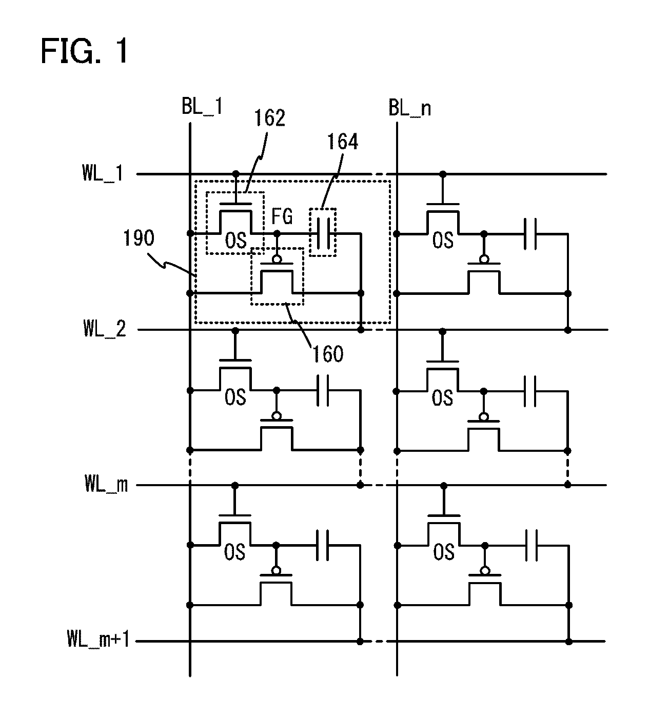
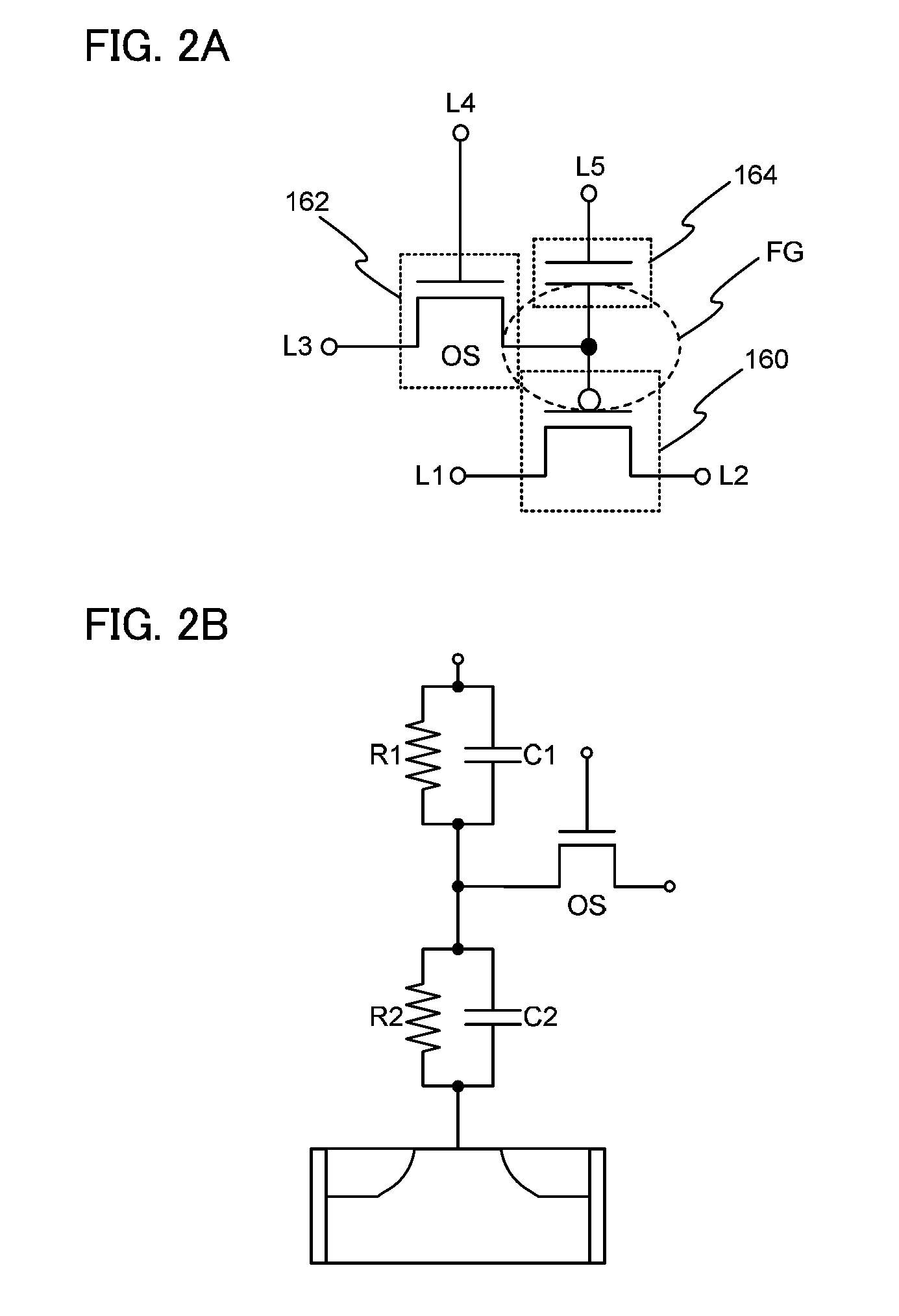
[0058]In this embodiment, a circuit configuration and operation of a semiconductor device according to one embodiment of the invention disclosed herein will be described with reference to the drawings. Note that in the circuit diagrams, “OS” may be written beside a transistor in order to indicate that the transistor includes an oxide semiconductor.

[0059]FIG. 1 illustrates an example of a circuit configuration of a semiconductor device according to one embodiment of the present invention. A structure including a first transistor 160, a second transistor 162, and a capacitor 164 is a memory cell 190. The structure in FIG. 1 includes n columns, and m memory cells 190 are included in each of the columns. Note that m and n are natural numbers.

[0060]Note that there is no particular limitation on the first transistor 160. In terms of increasing the speed of reading data, it is preferable to use, for example, a transistor with high switching rate, such as a transistor including single cryst...

embodiment 2

[0118]In this embodiment, a structure and a manufacturing method of a semiconductor device according to one embodiment of the invention disclosed herein will be described with reference to drawings.

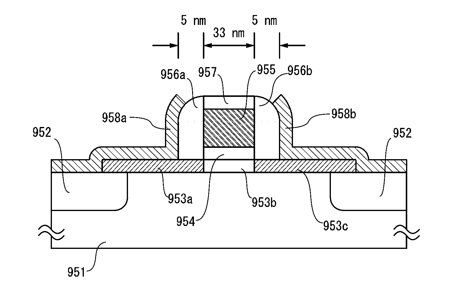
[0119]FIGS. 5A and 5B illustrate an example of the structure of the semiconductor device (the memory cell 190) illustrated in the circuit diagram of FIG. 1. FIGS. 5A and 5B are a cross-sectional view and a plan view, respectively, of the semiconductor device. Here, FIG. 5A corresponds to a cross section along line A1-A2 and line B1-B2 in FIG. 5B. Note that in FIG. 5B, wirings (electrodes) or the like are emphasized and insulating layers or the like are omitted for simple explanation.

[0120]In the semiconductor device illustrated in FIGS. 5A and 5B, the first transistor 160 including a first semiconductor material is included in a lower portion, and the second transistor 162 including a second semiconductor material is included in an upper portion.

[0121]Here, the first semiconductor materia...

embodiment 3

[0250]The actually measured field-effect mobility of an insulated gate transistor can be lower than its original mobility because of a variety of reasons; this phenomenon occurs not only in the case of using an oxide semiconductor. One of the reasons that reduce the mobility is a defect inside a semiconductor or a defect at an interface between the semiconductor and an insulating film. When a Levinson model is used, the field-effect mobility on the assumption that no defect exists inside the semiconductor can be calculated theoretically.

[0251]Assuming that the original mobility and the measured field-effect mobility of a semiconductor are μ0 and μ, respectively, and a potential barrier (such as a grain boundary) exists in the semiconductor, the measured field-effect mobility can be expressed as the following formula.

μ=μ0exp(-EkT)[FORMULA2]

[0252]Here, E represents the height of the potential barrier, k represents the Boltzmann constant, and T represents the absolute temperature. When...


PUM


Abstract

An object is to provide a semiconductor device which can hold stored data even when not powered and which achieves high integration by reduction of the number of wirings. The semiconductor device is formed using a material which can sufficiently reduce the off-state current of a transistor, e.g., an oxide semiconductor material which is a wide bandgap semiconductor. When a semiconductor material which allows a sufficient reduction in the off-state current of a transistor is used, data can be held for a long period. One line serves as the word line for writing and the word line for reading and one line serves as the bit line for writing and the bit line for reading, whereby the number of wirings is reduced. Further, by reducing the number of source lines, the storage capacity per unit area is increased.

Description

BACKGROUND OF THE INVENTION[0001]1. Field of the Invention[0002]The invention disclosed herein relates to a semiconductor device including a semiconductor element.[0003]2. Description of the Related Art[0004]Memory devices including semiconductor elements are broadly classified into two categories: volatile memory devices that lose stored data when not powered, and nonvolatile memory devices that hold stored data even when not powered.[0005]As a typical example of volatile memory devices, a dynamic random access memory (DRAM) is known. A DRAM stores data in such a manner that a transistor included in a storage element is selected and electric charge is stored in a capacitor.[0006]When data is read from a DRAM, electric charge in a capacitor is lost; thus, another write operation is necessary every time data is read out. Moreover, a transistor included in a memory element has leakage current (off-state current) between a source and a drain in an off state or the like and electric cha...

Claims


Application Information

Patent Timeline
IPC IPC(8): H01L27/108
CPCG11C16/0433H01L27/0207H01L27/11517G11C11/403H01L27/1211H01L27/1225H01L27/1156H10B41/00H10B41/70H10B99/00H10B12/00
Inventor MATSUBAYASHI, DAISUKE
Owner SEMICON ENERGY LAB CO LTD
Why Eureka
Try Eureka