Manufacturing method of semiconductor device

a manufacturing method and semiconductor technology, applied in the direction of semiconductor devices, basic electric elements, electrical equipment, etc., can solve the problems of difficult to achieve sufficient miniaturization at submicron level, short channel effect, and high probability of short channel effect, so as to achieve suppress defects and maintain favorable characteristics

Inactive Publication Date: 2012-02-09
SEMICON ENERGY LAB CO LTD
View PDF5 Cites 21 Cited by
  • Summary
  • Abstract
  • Description
  • Claims
  • Application Information

AI Technical Summary

Benefits of technology

[0048]By sufficiently reducing the size of the transistor, the area of a semiconductor device including the transistor is reduced, and the number of semiconductor devices obtained from one substrate is increased. Accordingly, the manufacturing cost per semiconductor device is reduced. Further, since the size of a semiconductor device is reduced, a semiconductor device having higher function than a conventional semiconductor device in almost the same size can be realized. Moreover, advantageous effects such as high-speed operation and lower power consumption due to a reduction in channel length can be obtained. In other words, according to one embodiment of the invention disclosed herein, miniaturization of a transistor including an oxide semiconductor is achieved, and therefore a variety of advantageous effects accompanying the miniaturization can be obtained.
[0049]As described above, according to one embodiment of the disclosed invention, a semiconductor device which suppresses defects or maintains favorable characteristics, and achieves miniaturization can be provided.

Problems solved by technology

In the case of using an exposure apparatus for glass substrates (also referred to as a stepper), the above-described limit of the feature size makes it difficult to achieve sufficient miniaturization at submicron level.
In the case where a transistor is miniaturized, a problem of a short channel effect arises.
The short channel effect is likely to occur particularly in a transistor including an oxide semiconductor because the threshold voltage of such a transistor cannot be controlled by doping, unlike a transistor including silicon.

Method used


Image

  • Manufacturing method of semiconductor device
  • Manufacturing method of semiconductor device
  • Manufacturing method of semiconductor device

Examples


embodiment 1

[0067]In this embodiment, a structure and a manufacturing method of a semiconductor device according to an embodiment of the invention disclosed herein will be described with reference to FIGS. 1A and 1B, and FIGS. 2A to 2E, FIGS. 3A to 3D, and FIGS. 4A to 4E.

Structure Example of Semiconductor Device

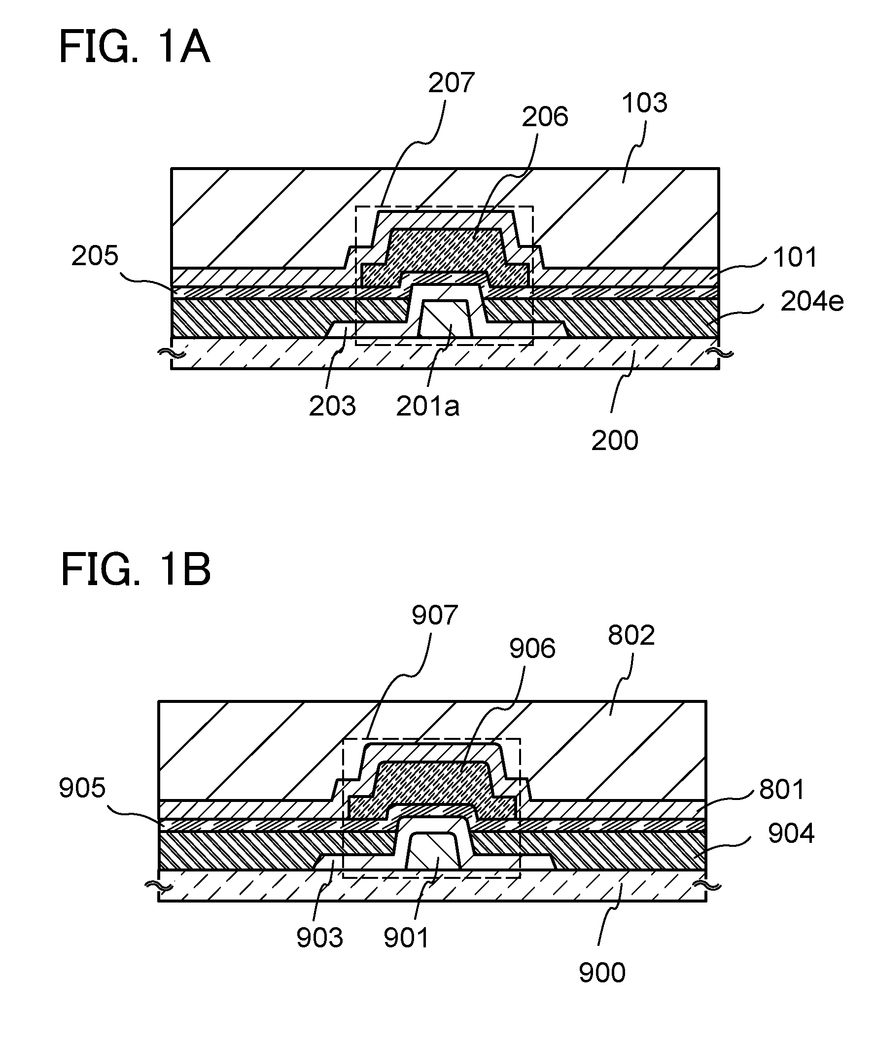
[0068]FIGS. 1A and 1B illustrate structure examples of a semiconductor device. FIG. 1A illustrates a first structure example, and FIG. 1B illustrates a second structure example.

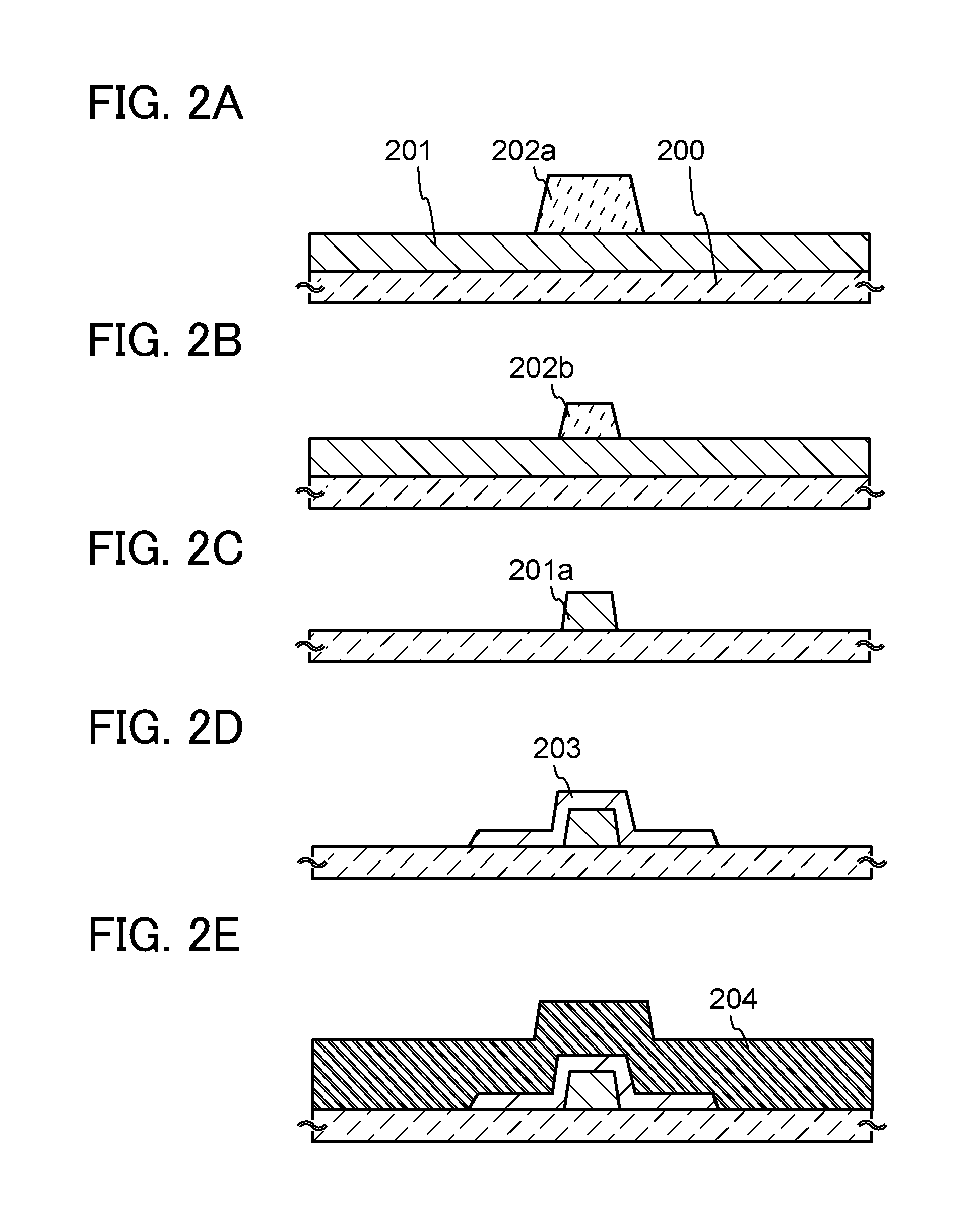
[0069]A transistor 207 illustrated in FIG. 1A includes an insulating layer 201a over a substrate 200 having an insulating surface, an oxide semiconductor layer 203 covering the insulating layer 201a, a conductive layer 204e functioning as a source electrode or a drain electrode, an insulating film 205 functioning as a gate insulating film, and a conductive layer 206 functioning as a gate electrode. The conductive layer 204e is in contact with a part of the oxide semiconductor layer 203 and a part of the substrate ...

embodiment 2

[0156]In this embodiment, a structure and a manufacturing method of a semiconductor device according to another embodiment of the invention disclosed herein will be described with reference to FIGS. 5A to 5C, FIGS. 6A to 6D, and FIGS. 7A to 7C.

Structure Example of Semiconductor Device

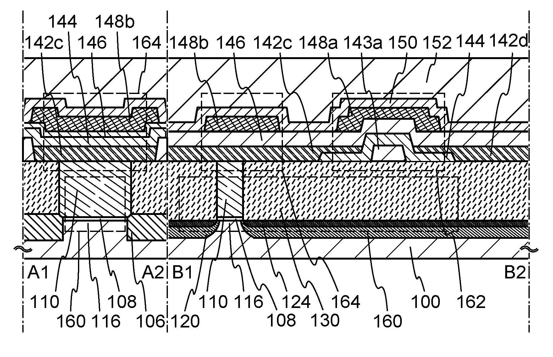
[0157]FIGS. 5A to 5C illustrate a structure example of a semiconductor device.FIG. 5A is a cross-sectional view of the semiconductor device; FIG. 5B is a plan view of the semiconductor device; and FIG. 5C illustrates a circuit configuration of the semiconductor device. Note that a structure of the semiconductor device is mainly described in this embodiment, and operation of the semiconductor device will be described in detail in the following embodiment. Note that the semiconductor device illustrated in FIGS. 5A to 5C is just an example of a semiconductor device having a predetermined function and does not exhaustively represent the semiconductor device of the invention disclosed herein. The semiconduct...

embodiment 3

[0189]In this embodiment, an example of application of a semiconductor device according to one embodiment of the invention disclosed herein will be described with reference to FIGS. 8A1, 8A2, and 8B. Here, an example of a memory device will be described. Note that in some circuit diagrams, “OS” is written beside a transistor in order to indicate that the transistor includes an oxide semiconductor.

[0190]In a semiconductor device which can be used as a memory device, which is illustrated in FIG. 8A1, a first wiring (1st Line) is electrically connected to a source electrode (or a drain electrode) of a transistor 1000. A second wiring (2nd Line) is electrically connected to a drain electrode (or a source electrode) of the transistor 1000. A third wiring (3rd Line) is electrically connected to a source electrode (or a drain electrode) of a transistor 1010. A fourth wiring (4th Line) is electrically connected to a gate electrode of the transistor 1010. Furthermore, a gate electrode of the...


PUM


Abstract

A semiconductor device in which a defect is suppressed and miniaturization is achieved is provided. An insulating film is formed over a flat surface; a first mask is formed over the insulating film; a second mask is formed by performing a slimming process on the first mask; an insulating layer is formed by performing an etching process on the insulating film using the second mask; an oxide semiconductor layer covering the insulating layer is formed; a conductive film covering the oxide semiconductor layer is formed; a surface of the conductive film is flattened by performing a polishing process on the conductive film; an etching process is performed on the conductive film, so that a conductive layer is formed and a surface of the conductive layer is lower than a surface of an uppermost part of the oxide semiconductor layer; a gate insulating film in contact with the conductive layer and the oxide semiconductor layer is formed; and a gate electrode is formed in a region which is over the gate insulating film and overlaps with the insulating layer.

Description

BACKGROUND OF THE INVENTION[0001]1. Field of the Invention[0002]The technical field of the present invention relates to a manufacturing method of a semiconductor device. Here, semiconductor devices refer to general elements and devices which function utilizing semiconductor characteristics.[0003]2. Description of the Related Art[0004]There are a wide variety of metal oxides and such metal oxides are used for various applications. Indium oxide is a well-known material and has been used for transparent electrodes required in liquid crystal display devices or the like.[0005]Some metal oxides have semiconductor characteristics. Examples of such metal oxides having semiconductor characteristics are tungsten oxide, tin oxide, indium oxide, zinc oxide, and the like. Thin film transistors in which a channel formation region is formed using such metal oxides are already known (e.g., see Patent Documents 1 to 4, Non-Patent Document 1, and the like).[0006]As metal oxides, not only single-compo...

Claims


Application Information

Patent Timeline
Patent Type & Authority Applications(United States)
IPC IPC(8): H01L21/336H01L21/283
CPCH01L29/78603H01L29/66969H01L29/78696H01L29/7869H01L27/1207H01L29/66742
Inventor SUZAWA, HIDEOMISASAGAWA, SHINYA
Owner SEMICON ENERGY LAB CO LTD
Why Eureka
Try Eureka