Photo-sensitive composite film, method of fabricating the same, and photo-switched device comprising the same

a composite film and photosensitive technology, applied in the direction of surface reaction electrolytic coating, discharge tube/lamp details, metal layered products, etc., can solve the problem of not having a large influence on the two-dimensional photoconductivity due to a few holes containing no metal nanoparticles therein, and achieve the effect of reducing the distance between the dielectric layer and the metal nanoparticles

Inactive Publication Date: 2012-02-16
NAT CHENG KUNG UNIV
View PDF1 Cites 6 Cited by
  • Summary
  • Abstract
  • Description
  • Claims
  • Application Information

AI Technical Summary

Benefits of technology

[0009]The photo-sensitive composite film of the present invention has a novel and simple structure, and can be manufactured by a simple method. In particular, the suitable activation wavelength for irradiation can be modified by altering the material of metal nanoparticles, the hole size of the anodized aluminum oxide film, and / or the size of the metal nanoparticles, and thus high variability is achieved. The photo-sensitive composite film according to the present invention has a quite simple structure and can be manufactured by a simple method, and the materials for preparing the composite film can be easily obtained. Therefore, the photo-sensitive composite film of the present invention is of great commercial value.
[0018]The photo-sensitive composite film according to the present invention has a quite simple structure and can be manufactured by a simple method, and the materials for preparing the composite film can be easily obtained. Therefore, the photo-sensitive composite film of the present invention is of great commercial value. In particular, the irradiation wavelength suitable for the photo-sensitive composite film of the present invention can be modified by altering the material of metal nanoparticles, and the hole size of the anodized aluminum oxide film, and thus high variability is achieved.
[0025]Preferably, the method for fabricating a photo-sensitive composite film according to the present invention further includes a step (F) after the step (D): thinning the anodized aluminum oxide film on the second surface to reduce the thickness of the aluminum oxide layer covering metal nanoparticles having been deposited at the bottom of the closed holes.
[0032]The photo-switched device of the present invention includes a photo-sensitive composite film with a novel and simple structure. The photo-sensitive composite film can be manufactured by a simple method. In particular, the suitable wavelength for irradiation can be modified by altering the material of metal nanoparticles, the hole size of the anodized aluminum oxide film, and / or the size of the metal nanoparticles, and thus high variability is achieved. The photo-switched device according to the present invention has a quite simple structure and can be manufactured by a simple method, and the materials for preparing the photo-switched device can be easily obtained. Therefore, the photo-switched device of the present invention is of great commercial value.

Problems solved by technology

However, the influence on two-dimensional photoconductivity due to a few holes containing no metal nanoparticles therein is not great.

Method used


Image

  • Photo-sensitive composite film, method of fabricating the same, and photo-switched device comprising the same
  • Photo-sensitive composite film, method of fabricating the same, and photo-switched device comprising the same
  • Photo-sensitive composite film, method of fabricating the same, and photo-switched device comprising the same

Examples


example 1

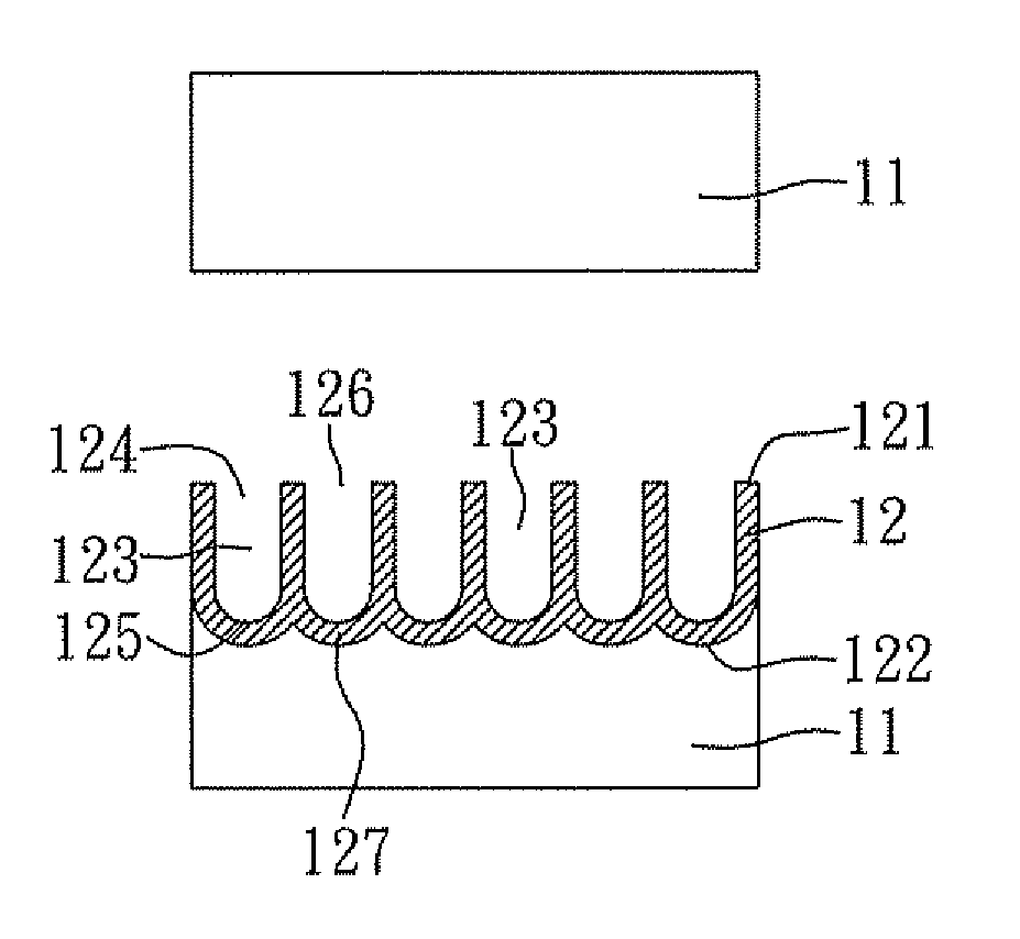
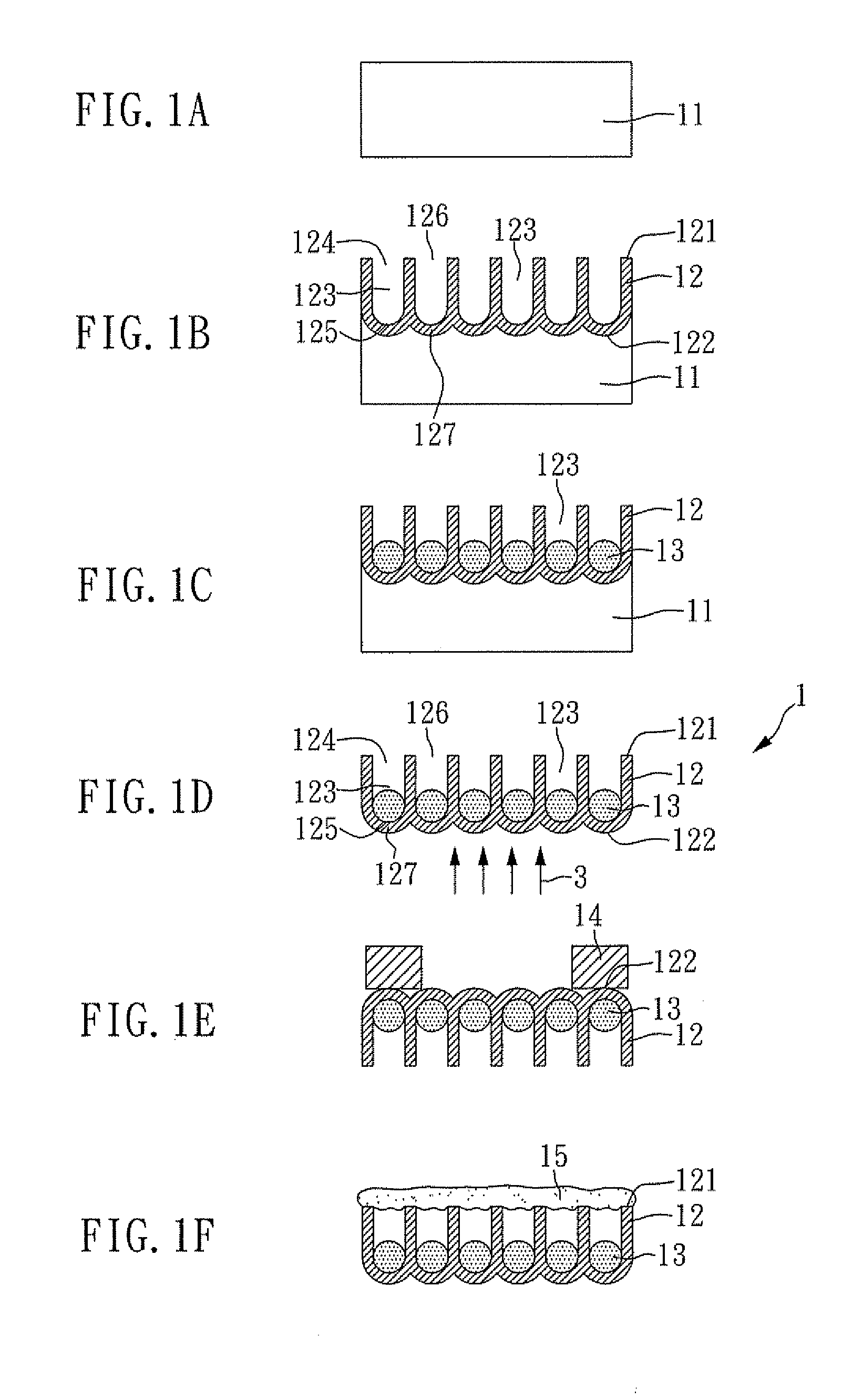
[0047]FIGS. 1A to 1D show a process to manufacture a photo-sensitive composite film according to the present example. As shown in FIG. 1A, an aluminum plate 11 is first provided in the step (A). Then, as shown in FIG. 1B, the aluminum plate 11 is subjected to an anodizing treatment to form an aluminum oxide film 12 on the surface of the aluminum plate 11 in the step (B). The film 12 is made of a porous material with nano-pores, and has a first surface 121 and a second surface 122 opposite to the first surface 121. In addition, the anodized aluminum oxide film 12 has a plurality of long tube shaped holes 123. Each of the holes 123 has a first end 124 and a second end 125. The first end 124 has an opening 126 at the first surface 121 of the anodized aluminum oxide film 12, while the second end 125 of the hole 123 is closed and located at the second surface 122 of the anodized aluminum oxide film 12. The closed second end 125 is covered by an aluminum oxide layer 127. Subsequently, as ...

example 2

[0051]The photo-sensitive composite film according to the present example is manufactured by the same process as illustrated in Example 1, except that gold metal nanoparticles (rather than silver metal nanoparticles) are grown in the holes of the anodized aluminum oxide film under a voltage of 45 V in the step (C). Since the material of the metal nanoparticles in the holes according to the present example is different from that of Example 1, the light wavelength required by the photo-sensitive composite film according to the present example to induce conductivity is different from that required in Example 1.

example 3

[0052]After a photo-sensitive composite film 1 is manufactured by the same method as illustrated in Example 1, a step (D1) of forming two electrodes 14 on the second surface 122 of the anodized aluminum oxide film 12 is performed, as shown in FIG. 1E. These electrodes 14 can provide the photo-sensitive composite film 1 with external electrical connection.


PUM

PropertyMeasurementUnit
diameteraaaaaaaaaa
voltageaaaaaaaaaa
voltageaaaaaaaaaa

Abstract

A photo-sensitive composite film is disclosed, which includes plural metal nano-particles and a porous anodized aluminum oxide film. The nanoparticles can be hollow or solid with unrestricted shapes of varying diameters and lengths. The plural metal nanoparticles are completely contained in holes and attached to the bottom of the holes of the anodized aluminum oxide film, and the electrical conductivity of the photo-sensitive anodized aluminum oxide film can be changed by light exposure on the metal nanoparticles from surfaces of the anodized aluminum oxide film. The structure of the photo-sensitive anodized aluminum oxide film of the present invention is uncomplicated and the manufacturing steps thereof are simple, and therefore the photo-sensitive anodized aluminum oxide film of the present invention is of great commercial value. Also, a method of manufacturing the above photo-sensitive composite film and a photo-switched device including the same are disclosed.

Description

CROSS REFERENCE TO RELATED APPLICATION[0001]This application claims the benefits of the Taiwan Patent Application Serial Number 099127349, filed on Aug. 16, 2010, and the Taiwan Patent Application Serial Number 099132361, filed on Sep. 24, 2010, the subject matters of which are incorporated herein by reference.BACKGROUND OF THE INVENTION[0002]1. Field of the Invention[0003]The present invention relates to a photo-sensitive composite film, a method for fabricating the same and a photo-switched device comprising the same, more particularly, to a photo-sensitive composite film comprising a plurality of metal nanoparticles and an anodized porous aluminum oxide film, a method for fabricating the same and a photo-switched device comprising the same.[0004]2. Description of Related Art[0005]Photoconductivity is a phenomenon in which a material has enhanced electrical conductivity (or reduced resistance) due to the absorption of specific spectra upon being irradiated by light. Photo-sensitiv...

Claims


Application Information

Patent Timeline
Patent Type & Authority Applications(United States)
IPC IPC(8): H03K17/78B32B15/02C25D1/00B32B5/18B32B9/04B82Y30/00B82Y40/00
CPCB82Y30/00B82Y40/00C25D11/18C25D15/00H03K17/941H03K2217/94106C25D11/045C25D1/006Y10T428/24997
Inventor TZENG, YON-HUALIU, CHIH-YIKYAW, KYAW-OOCHUI, HSIANG-CHENHUANG, CHEN-HANLIN, HSING-YING
Owner NAT CHENG KUNG UNIV
Why Eureka
Try Eureka