Dynamic nano-inscribing for continuous and seamless metal and polymer nanogratings

a nano-grating and nano-inscribing technology, applied in the field of nanofabrication techniques, can solve the problems of insufficient wafer, insufficient process and throughput of nil, damage to sensitive resist materials, etc., to achieve more faithful polymer patterns, reduce the modulus of materials, and enhance toughness

Active Publication Date: 2012-02-16
RGT UNIV OF MICHIGAN
View PDF1 Cites 8 Cited by
  • Summary
  • Abstract
  • Description
  • Claims
  • Application Information

AI Technical Summary

Benefits of technology

[0033]Even though Dynamic Nano-Inscribing can be performed in most cases under the ambient environment, heating of the polymer layer 18 during the inscribing process can effectively reduce the modulus of the material and enhance its toughness, which can lead to more faithful polymer patterns. However, bulk heating of the whole substrate results in significant pattern deformation due to polymer flow at elevated temperatures. Therefore, according to the principles of the present teachings, conductive heating of the Si mold 14 can be used to localize the heating to only a very small region of the moving substrate where the Si mold 14 is engaged. Such localized heating allows the patterned structure to quickly cool down after the inscription, and also does not affect the inscribed structures away from the mold contact region. As illustrated in FIG. 4a, the localized heating-assisted Dynamic Nano-Inscribing (LH-DNI) is provided. The Si mold 14 can be directly heated by a heating element 30 with temperature controller (HOTSET Inc.). As shown in FIG. 4b, the pattern depth in the polycarbonate / polymer layer 18 increases with temperature under the same applied force (4.2 N) and web speed (2.5 mm / sec) conditions. Polycarbonate nano gratings fabricated at room temperature (RT-DNI) show a shallow and rounded profile (FIG. 4c), while the sample fabricated by localized heating-assisted Dynamic Nano-Inscribing at 140° C., a temperature slightly lower than the Tg of polycarbonate (150° C.), shows much deeper trenches and sharper edges, representing a more faithful replication (FIG. 4d) of the grating structure on the original mold (FIG. 4e).
[0034]In localized heating-assisted Dynamic Nano-Inscribing, even though heat is applied, the actual time for heat transfer to the substrate is only on the order of tens of microseconds, which is several orders of magnitude shorter than the heating time used in a typical thermal NIL process. This can drastically minimize any potential damage to thermal sensitive materials. Applicant has demonstrated Dynamic Nano-Inscribing on conductive polymer, poly(3,4-ethylenedioxythiophene) (PEDOT) and an organic semiconductor—conjugated polymer poly(3-hexylthiophene) (P3HT), which are representative materials commonly used in organic electronics and organic optoelectronics. It has been found that nano patterned P3HT in organic photovoltaics shows enhanced light absorption and an increase in overall solar cell efficiency. In addition, various techniques have been explored to pattern micro or nano structures on P3HT and PEDOT for applications in organic photovoltaics, organic TFTs and organic LEDs. Compared to these referenced techniques, Dynamic Nano-Inscribing provides superior throughput and a simple one-step process for patterning organic functional materials while minimizing possible thermal damage. FIGS. 4f and 4g show 700 nm period nano gratings directly created on PEDOT and P3HT coated PET respectively by localized heating-assisted Dynamic Nano-Inscribing at 90° C.
[0035]It has also been found that the Dynamic Nano-Inscribing process of the present teachings can be completed in an oxygen-free environment to prevent the oxidation effect and further preserve the functionality of the conjugated polymers. A potential application is in the field of organic solar cells, where Dynamic Nano-Inscribing could be used to directly inscribe conjugated polymers to produce the ordered nanoscale interface between a donor and an acceptor organic semiconductors for efficient charge separation and charge transport.
[0036]As another example of patterning functional polymers, Nano-inscribing of Nafion film (DuPont), an important polymer material in electrochemistry, has been explored. Nafion film serves an important role as the ion exchange membrane in fuel cells due to its excellent proton conductivity, and its thermal and mechanical stability. Recently it has been reported that nano patterning of Nafion can provide enhanced efficiency in micro-fuel cells by increasing the electrochemical active surface areas. In FIG. 4h, well defined 700 nm period gratings are created in Nafion film by a simple Dynamic Nano-Inscribing process using localized heating at 80° C.
[0037]Finally as an application in photonics, it has been found that a metallic grating fabricated by a one-step Dynamic Nano-Inscribing can be used to construct negative refractive index metamaterials. Negative refraction requires a simultaneously negative permittivity and permeability. While negative permittivity is readily achievable in metallic structures due to plasmon dispersion, negative permeability can only be obtained in specially designed artificial structures. Previously, several variations of the so-called split-ring resonator (SRR) structures have been exploited to produce magnetic response and negative permeability. Recently an elongate SRR structure has been demonstrated by using direct laser writing and silver chemical vapor deposition, which offers the advantage of normal incidence. To produce magnetic response and negative permeability at shorter wavelength ranges (e.g. visible band), the dimension of the subwavelength element in the structure has to be reduced accordingly. A Split-Ring-Resonant-Grating (SRRG) structure fabricated by nanoimprinting and metal film deposition was studied, which showed the potential of achieving negative refraction at visible wavelengths.
[0038]According to the present teachings, one can fabricate 200 nm period (30 nm trench) SRRG structure using the Dynamic Nano-Inscribing process (FIG. 5a). To achieve this structure, 20 nm thick silver is thermally deposited on a polycarbonate film and simply inscribed using a 200 nm period Si mold at room temperature. FIG. 5b shows the transmittance spectra of the sample of FIG. 5a for both TM (transverse magnetic) and TE (transverse electric) polarization, showing particularly strong TM mode transmission valleys at visible wavelength range of 430 nm and 590 nm. Based on simulation, it was determined that the valley at 430 nm is due to electrical resonance while the valley at 590 nm is due to magnetic resonance and leads to negative permeability. Further optimization of the structure to demonstrate negative index at visible band is currently underway. As compared with NIL and other nano fabrication techniques, Dynamic Nano-Inscribing provides a very simple, single step process to create large area continuous nano metal grating patterns for negative index metamaterial applications.

Problems solved by technology

Unfortunately, the current process and throughput of NIL, which is on the order of a few minutes per wafer, is insufficient to meet the currently demands of many practical applications, such as photonics, biotechnology, and organic optoelectronics.
Unfortunately, the UV or high temperature heating process inherent in R2RNIL may damage sensitive resist materials.
Moreover, the method of R2RNIL results in an unavoidable seam region where the two ends of the flexible mold meet on the roller.
This unavoidable seam region interrupts the otherwise continuous patterns.
Still further, it has been difficult to fabricate the large area original imprint molds that are used in R2RNIL to replicate flexible stamps.

Method used


Image

  • Dynamic nano-inscribing for continuous and seamless metal and polymer nanogratings
  • Dynamic nano-inscribing for continuous and seamless metal and polymer nanogratings
  • Dynamic nano-inscribing for continuous and seamless metal and polymer nanogratings

Examples


Embodiment Construction

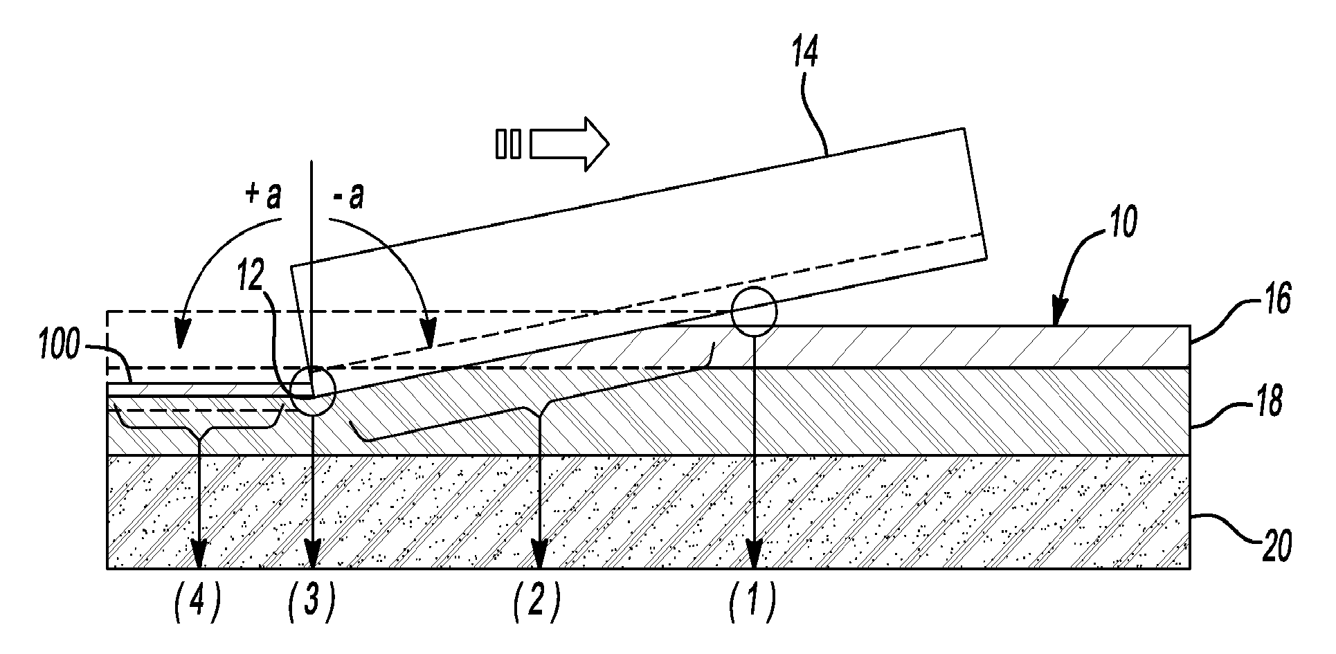
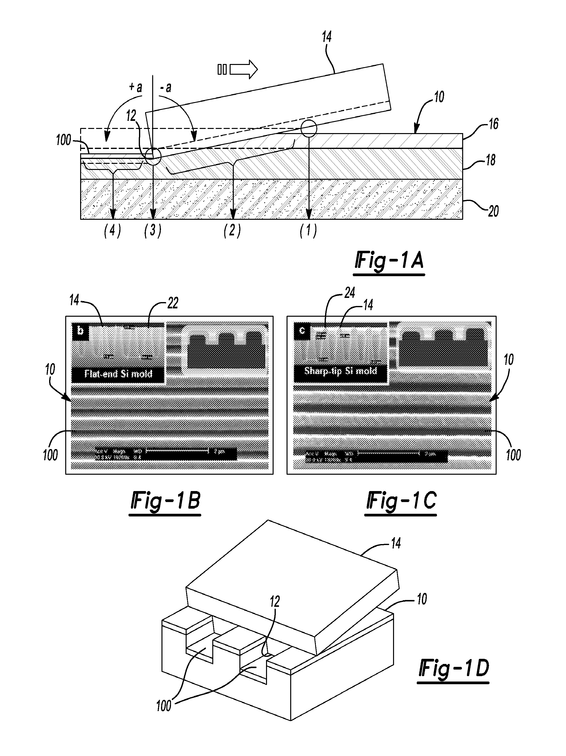
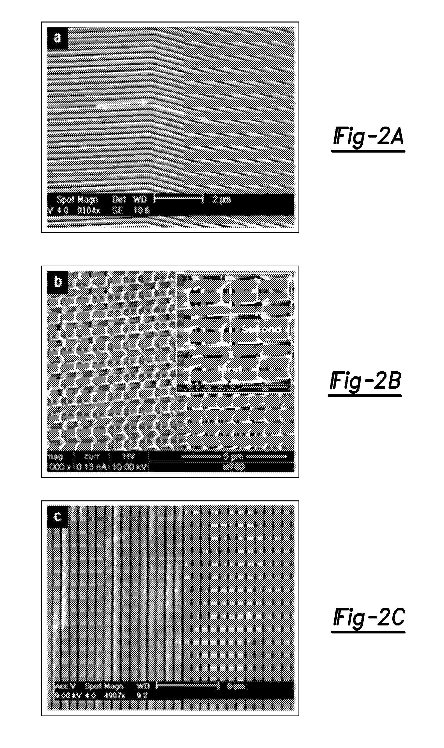
[0016]Embodiments are provided so that this disclosure will be thorough, and will fully convey the scope to those who are skilled in the art. Numerous specific details are set forth such as examples of specific components, devices, and methods, to provide a thorough understanding of embodiments of the present disclosure. It will be apparent to those skilled in the art that specific details need not be employed, that example embodiments may be embodied in many different forms and that neither should be construed to limit the scope of the disclosure.

[0017]The terminology used herein is for the purpose of describing particular example embodiments only and is not intended to be limiting. As used herein, the singular forms “a”, “an” and “the” may be intended to include the plural forms as well, unless the context clearly indicates otherwise. The terms “comprises,”“comprising,”“including,” and “having,” are inclusive and therefore specify the presence of stated features, integers, steps, ...


PUM

PropertyMeasurementUnit
outer diameteraaaaaaaaaa
temperatureaaaaaaaaaa

Abstract

Nanoscale grating structure can be utilized in many practical applications in optics, flat-panel displays and bio-sensors. A Dynamic Nano-Inscribing (Dynamic Nano-Inscribing) technique is disclosed for directly creating large-area, truly continuous nano-grating patterns in a variety of metal or polymer materials with feature size down to sub-50 nm and at very high speed (10 cm/sec). Dynamic Nano-Inscribing is carried out under either ambient temperature or with a brief heating time on the order of ten microseconds, which minimizes damage on UV or thermo-sensitive functional materials.

Description

CROSS-REFERENCE TO RELATED APPLICATIONS[0001]This application claims the benefit of U.S. Provisional Application No. 61 / 169,398 filed on Apr. 15, 2009. The entire disclosure of the above application is incorporated herein by reference.GOVERNMENT INTEREST[0002]This invention was made with government support under Grant No. 0700718 awarded by the National Science Foundation. The government has certain rights in the inventionFIELD[0003]The present disclosure relates to nanofabrication techniques and, more particularly, relates to a dynamic nano inscribing process and apparatus for nanofabrication.BACKGROUND AND SUMMARY[0004]This section provides background information related to the present disclosure which is not necessarily prior art. This section also provides a general summary of the disclosure, and is not a comprehensive disclosure of its full scope or all of its features.[0005]The increasing demands for nano-scale grating and channel structures in optics and bio-industries have s...

Claims


Application Information

Patent Timeline
Patent Type & Authority Applications(United States)
IPC IPC(8): B29C59/02B82Y40/00
CPCB82Y20/00G02B5/1809G02B5/1852G02B2207/101
Inventor AHN, SE HYUNGUO, LINGJIE JAY
Owner RGT UNIV OF MICHIGAN
Why Eureka
Try Eureka