
Semiconductor device

Inactive Publication Date: 2012-02-16
SONY CORP
View PDF3 Cites 12 Cited by
  • Summary
  • Abstract
  • Description
  • Claims
  • Application Information

AI Technical Summary

Benefits of technology

[0011]It is unavoidable that the word line capacity becomes extremely large, since it is necessary to flow a large current in writing operation. However, this has a negative impact on reading operation. Specifically, at the time of reading operation, it is not necessary to increase electric potential of the word line compared to at the time of writing operation. Thus, in some cases, the reading voltage applied to the word line at the time of reading is lower than the programming voltage applied to the word line at the time of writing. In reality, since it is necessary to read the storage data while retaining the resistance value changed by writing operation, the reading voltage is lower than the programming voltage. However, in the case where the word line with a large capacity is driven at a low voltage, access time is increased. Further, since the word line capacity is extremely large, excessive power is consumed at the time of charging and discharging the word line, which is an inhibitory element of incapability of reducing power consumption of semiconductor devices.
[0012]In the case where the access time at the time of reading is long and desired operation time is not satisfied as described above, the number of memory cells (storage bit count) connectable per one word line is limited. In some cases, such limitation of the number of memory cells occurs similarly in the case where the memory power consumption is excessively large due to needs of a system on which the relevant memory is installed. Accordingly, trade-off relation exists between decreasing the access time and the power consumption and improving the storage bit count per one word line.
[0016]According to the foregoing configuration, the plurality of cell transistors that are connected in parallel with each other are included for every memory cell. Thus, the current flown to the storage device is able to be optimally controlled at the time of operation. For example, in the case where a current value necessary for the case of date storage is larger than a current value necessary at the time of reading data, the number of cell transistors turned ON at the time of data storage is able to be larger than that at the time of reading data. Therefore, the total operation time is decreased down to the very minimum. Further, in operation to turn ON only the necessary number of cell transistors out of the plurality of cell transistors, power consumption is decreased more than that of operation to turn ON all the cell transistors. Meanwhile, since operation time and power consumption are decreased, the number of memory cells concurrently driven is able to be increased.
[0017]According to the present invention, a semiconductor memory device in which trade-off between decreasing the access time and the power consumption and improving the storage bit count per one word line is resolved or modified is able to be provided.

Problems solved by technology

Thus, in the case where a size of each access transistor is large, capacity of the word line (comprehensive capacity of wiring capacity and load capacity) becomes extremely large.
It is unavoidable that the word line capacity becomes extremely large, since it is necessary to flow a large current in writing operation.
However, this has a negative impact on reading operation.
Further, since the word line capacity is extremely large, excessive power is consumed at the time of charging and discharging the word line, which is an inhibitory element of incapability of reducing power consumption of semiconductor devices.
In some cases, such limitation of the number of memory cells occurs similarly in the case where the memory power consumption is excessively large due to needs of a system on which the relevant memory is installed.

Method used


Image

  • Semiconductor device
  • Semiconductor device
  • Semiconductor device

Examples


first embodiment

1. First Embodiment

Chip Configuration

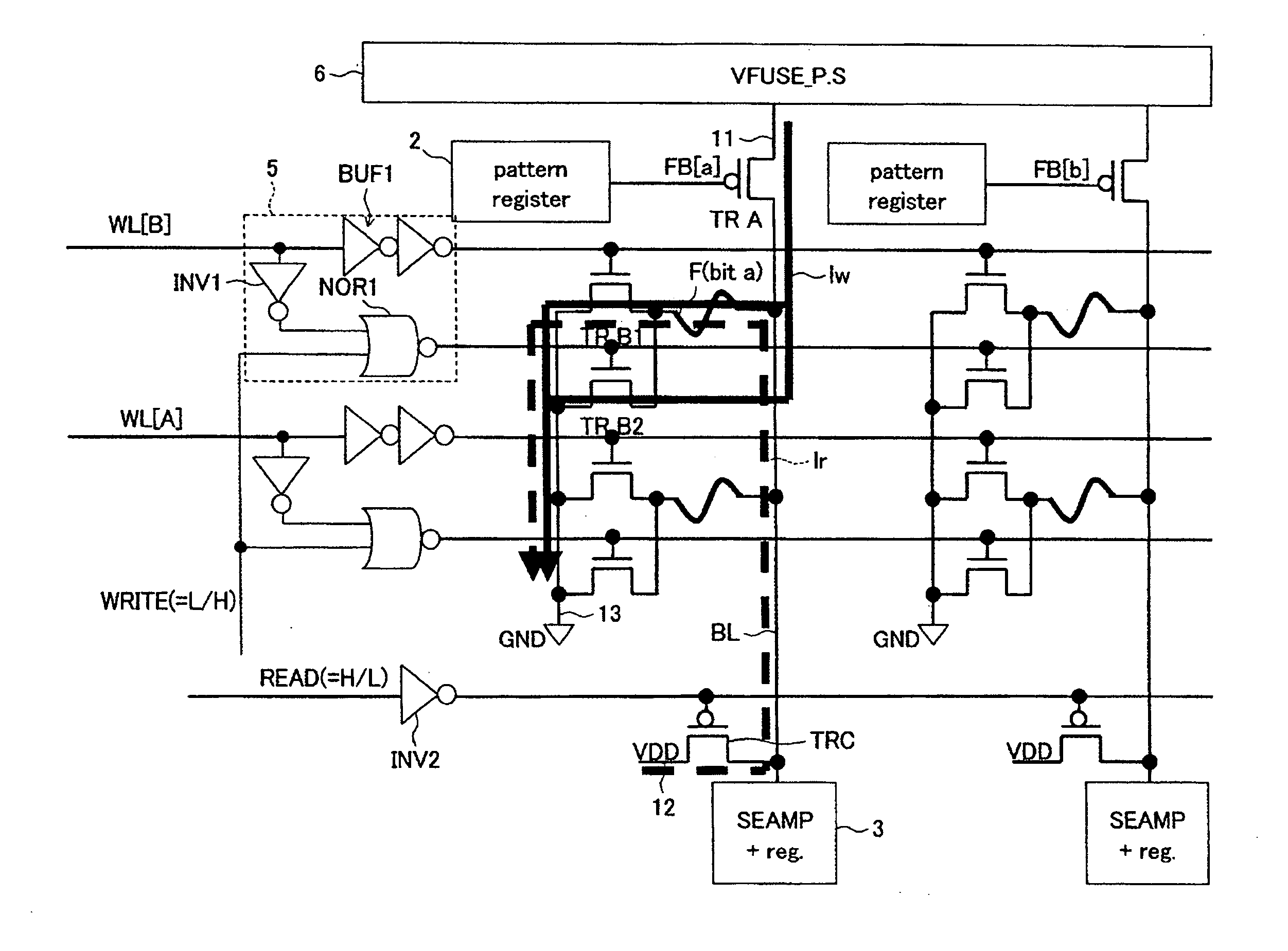
[0026]FIG. 1 illustrates a chip configuration diagram of a semiconductor device according to the first embodiment. The semiconductor device of this embodiment includes a memory cell array 1 and various control circuits for controlling programming (writing) and reading of the memory cell array 1.

[0027]In the memory cell array 1, a plurality of memory cells MC are arranged in a matrix state. As described later, each of the memory cell MC is provided between a bit line BL and a third voltage supply line (GND line 13), and, for example, has a fuse device F and an access transistor TRB serially connected to the fuse device F. FIG. 1 exemplifies a case that four memory cells MC are arranged in two columns (2 bits)×2 rows. However, arrangement of the plurality of memory cells MC is not limited to the arrangement of FIG. 1, and for example, the plurality of memory cells MC may be arranged in one row. It is to be noted that, in the following description, ...

second embodiment

2. Second Embodiment

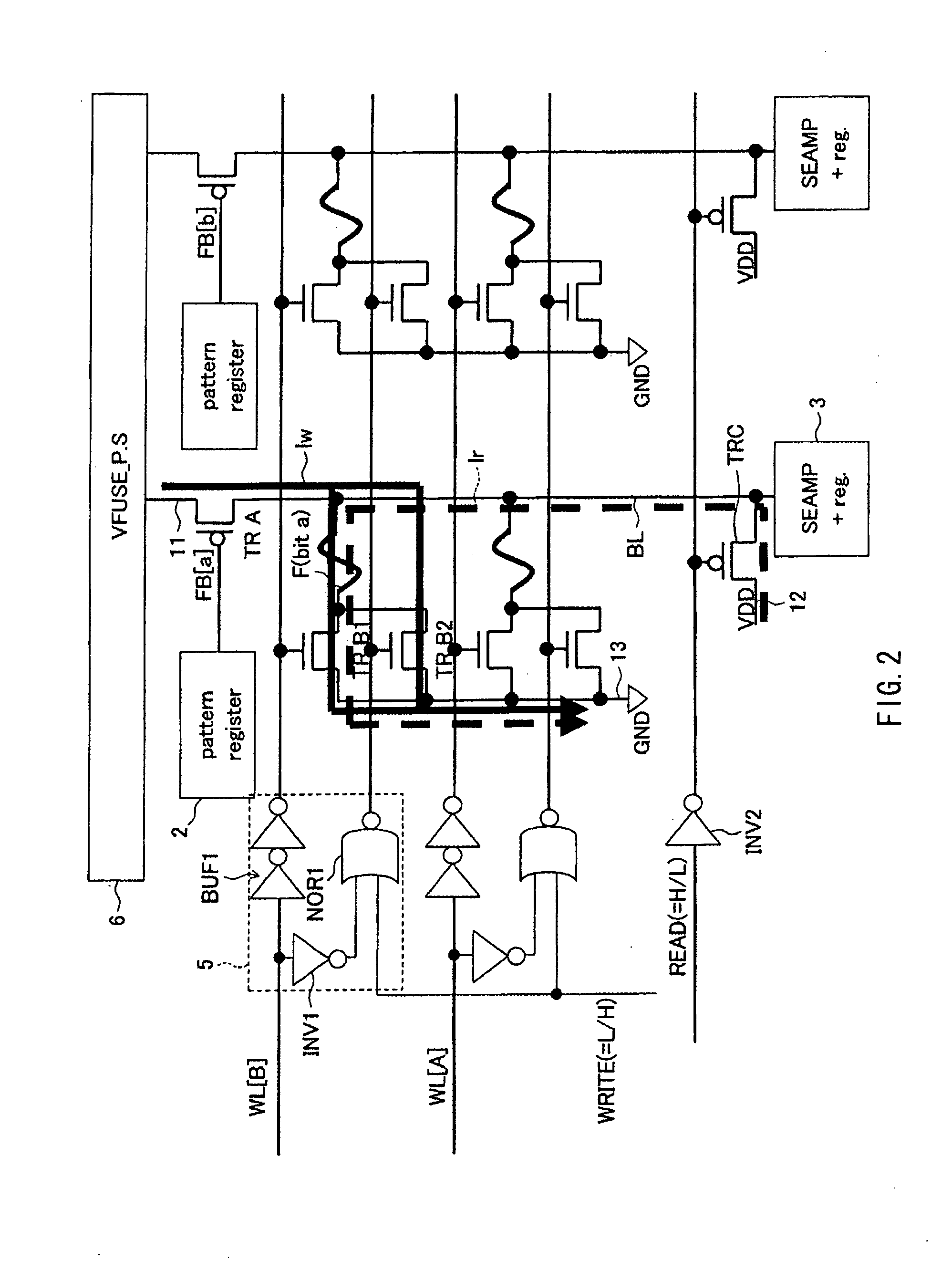
[0100]FIG. 4 illustrates a chip configuration diagram of a semiconductor device according to the second embodiment. Further, FIG. 5 illustrates a path of a current flown at the time of operation. A description will be given of difference between FIGS. 4 and 5 and FIGS. 1 and 2 according to the first embodiment. In FIGS. 4 and 5, descriptions of the elements affixed with the same referential numbers as those of FIGS. 1 and 2 will be omitted.

[0101]In this embodiment, the access transistor TRB is composed of three cell transistors, that is, the first cell transistor TRB1, the second cell transistor TRB2, and a third cell transistor TRB3. The first, the second, and the third cell transistors TRB1, TRB2, and TRB3 are each composed of an NMOS transistor, and are connected to each other in parallel.

[0102]In this embodiment, the first cell transistor TRB1 is a cell transistor that is constantly used (is turned ON) at the time of reading and at the time of programming (he...


PUM


Abstract

Both decreasing access time and power consumption and improving storage bit count per one word line are compatibly attained. A memory cell array 1 has a configuration in which at least one row of memory cells MC having a fuse device F with a resistance value variable according to a flowing current and a plurality of cell transistors (TRB1 and TRB2) connected in parallel with respect to the fuse device F is arranged. In the relevant semiconductor device, out of the plurality of cell transistors (TRB1 and TRB2), the number of cell transistors turned ON is controllable by a writing control signal (WRITE) inputted from outside and an internal logic circuit 5 (and a word line drive circuit 4).

Description

TECHNICAL FIELD[0001]The present invention relates to a semiconductor device that has a memory cell having a storage device with a resistance value variable according to a flowing current and a cell transistor for accessing the same in a memory cell array.BACKGROUND ART[0002]As a representative storage device with a resistance value variable according to a flowing current, a resistance random access memory device and a fuse device are known. The resistance random access memory device is a memory device using conductivity change according to input / output of conductive ions to / from an insulating film and magnetization direction of a magnetic film, phase change of a crystal structure and the like, and is able to reversibly change a resistance value.[0003]Meanwhile, as the fuse device, in addition to a fuse device which is burned out by laser light, for example, a fuse device that controls the resistance value by electrically melting down a fuse made of polysilicon is known (for example...

Claims


Application Information

Patent Timeline
IPC IPC(8): G11C17/16
CPCG11C13/0004G11C13/003G11C17/16G11C17/18G11C2213/74G11C2213/79H01L27/105H01L27/112H01L27/11206H01L27/11286H10B20/00H10B20/20H10B20/60G11C17/14G11C13/00
Inventor TORIGE, YUJI
Owner SONY CORP
Learn More