[0005]
Cell access operation of RAM is described as follows. While Reading data of a data storage node in a cell, a bit-line corresponding to the
data node is first pre-charged to
high voltage of logic 1. When Reading starts, the data storage node of the cell is connected to the bit-line by a corresponding pass-gate
transistor; if the data storage node stores logic 0 of
low voltage, the
inverter in the cell pulls down the voltage of the bit-line to reflect stored data of logic 0. Before Reading starts, an n-channel MOS
transistor in the
inverter pulls down and hold the data storage node to
low voltage so the data storage node can store logic 0. As Reading starts, however, voltage at the data storage node will be raised because the data storage node is connected to the bit-line which is at
high voltage. Equivalently, the pass-gate
transistor and the n-channel MOS transistor in the
inverter form a
voltage divider between high bit-line voltage of logic 1 and
low voltage of logic 0 as Reading starts. If voltage at the data storage node is raised too high, it will exceed a trip voltage of the opposite inverter in the latch structure, and data of the data storage node will be incorrectly flipped from logic 0 to logic 1 by feedback mechanism of the latch structure. To prevent incorrect data flip during Read, weak pass-gate transistors (with narrower width or longer channels, lower conduction and larger source-
drain resistance) are adopted in cells; whereas relatively strong (lower source-
drain resistance) n-channel MOS transistors are used, such that the voltage at the data storage node will be contained to below the trip voltage of the opposite inverter to improve
noise margin during Read.
[0007]In other words, requirements for data Read and data Write are mutually conflicting; and the conflict is more severe for compact
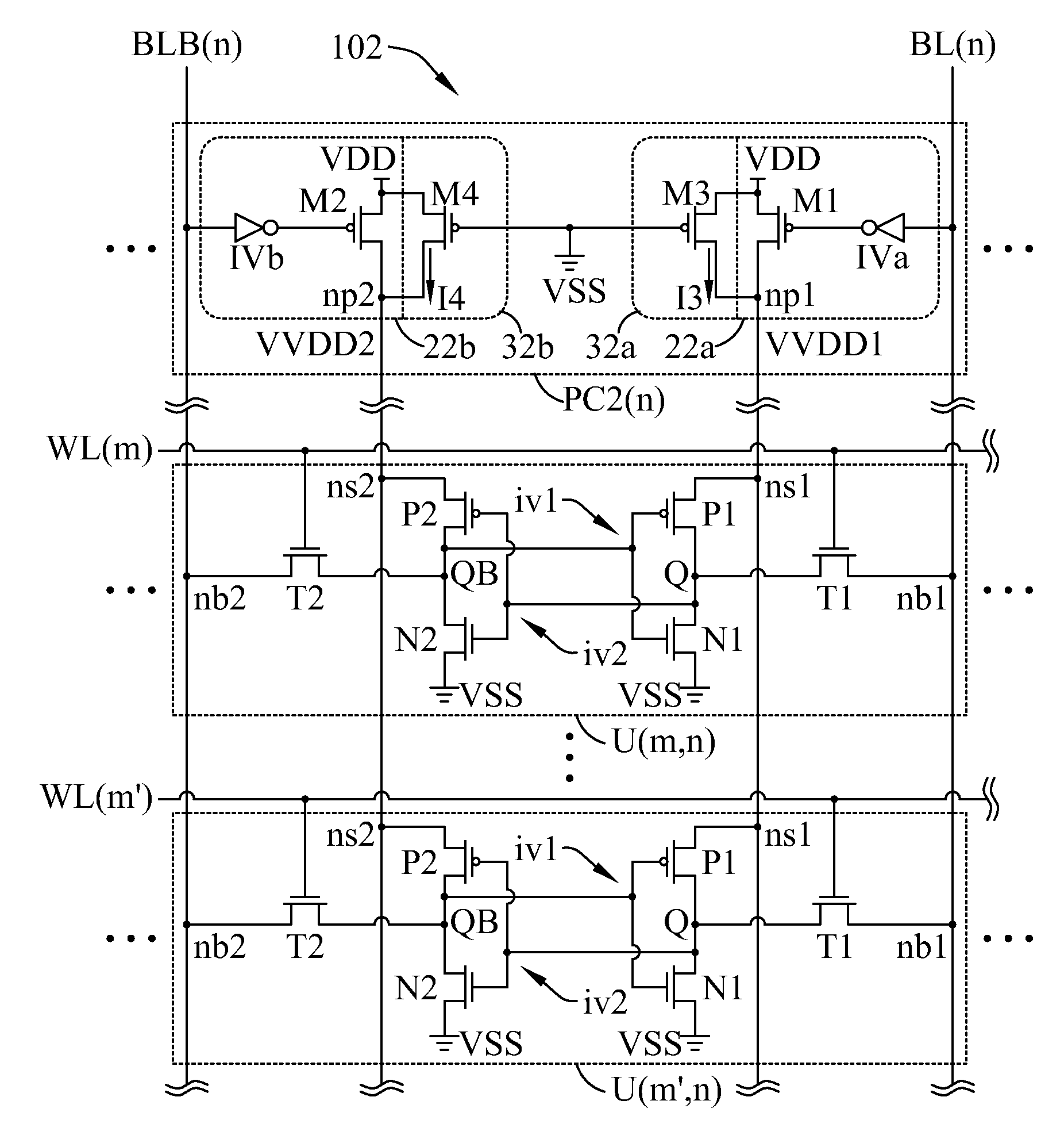
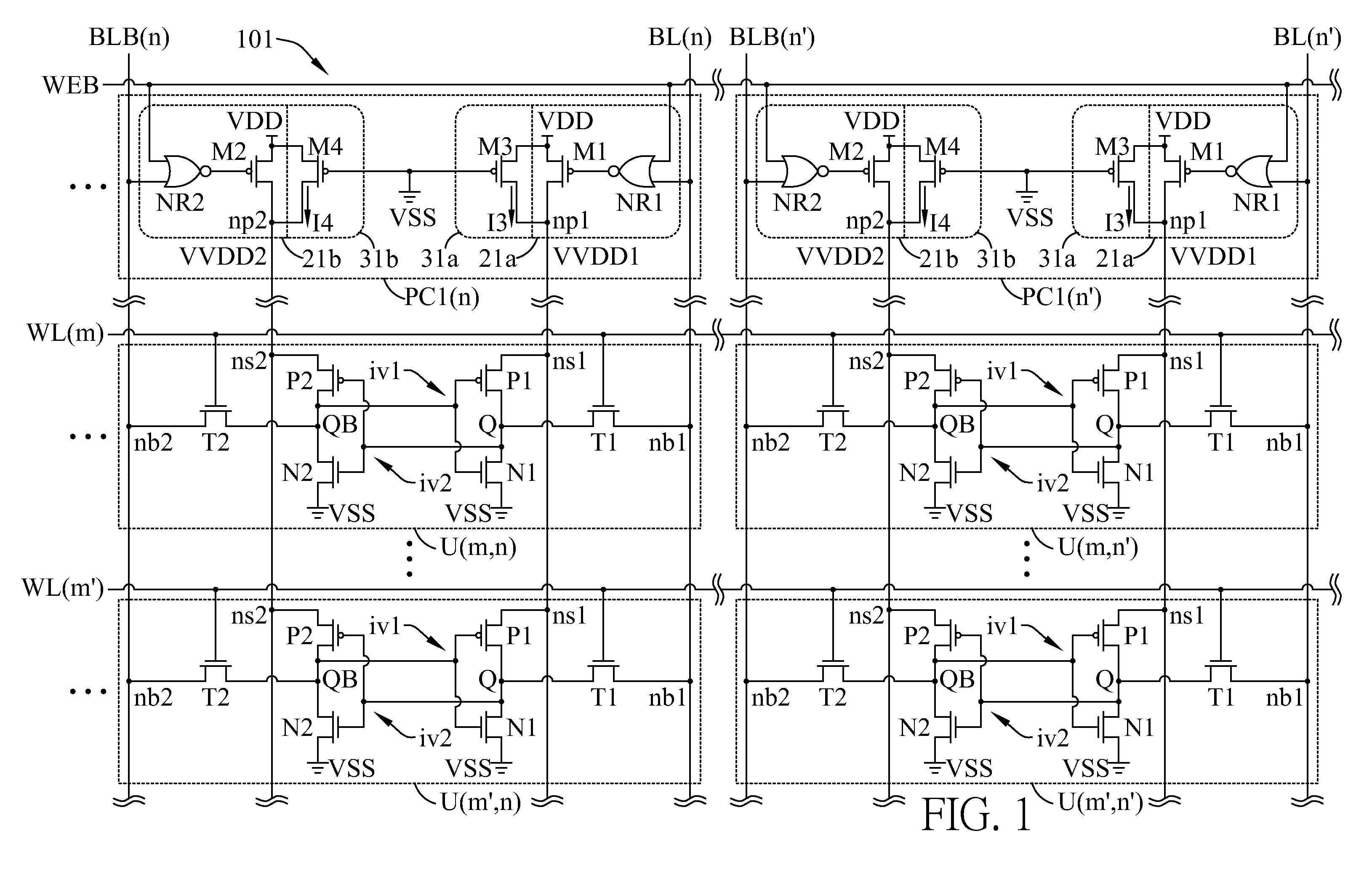
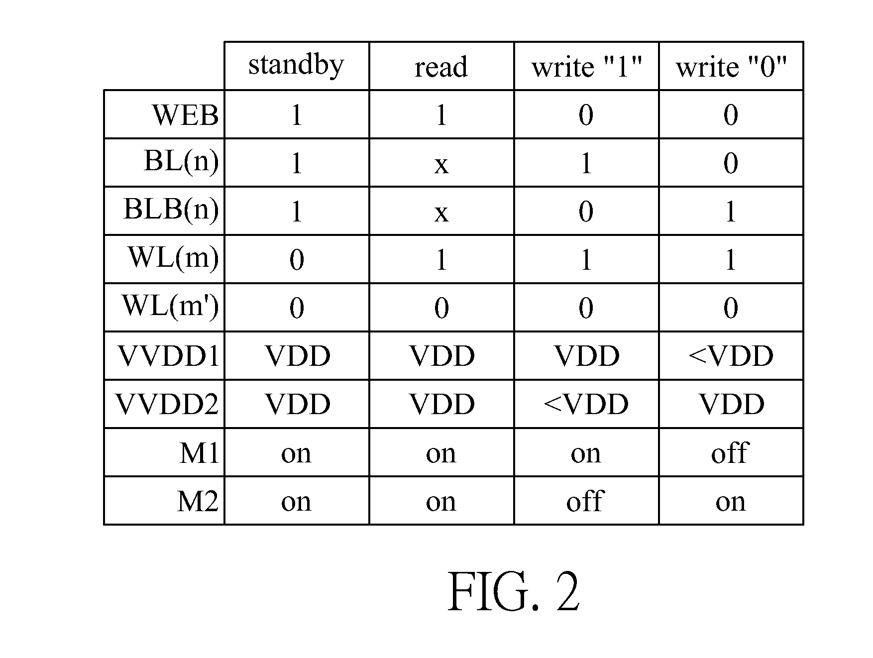
layout / low operation voltage RAM / cell in advanced / scaled process. To mitigate the conflict of Read and Write operation, a RAM, with column-based independent supply controls for the two respective inverters in each cell of a column according to data voltages of bit-lines, is disclosed. In the disclosure of the invention, weak pass-gate transistors can be adopted to reduce Read disturb and improve Read
Static Noise Margin (RSNM). To improve Write-ability and Write performance, when logic 0 is written to a data storage node originally storing logic 1, assuming the data storage node is held at
high voltage (logic 1) by a p-channel MOS transistor of a first inverter, then, during Write operation, the power supply control of invention will reduce the source supply voltage of the p-channel MOS transistor of the first inverter, but maintain the source supply voltage of the p-channel MOS transistor of the opposite (second) inverter in the cell. Reducing source supply voltage of the p-channel MOS transistor of the first inverter lowers the Source-to-
Gate voltage of the p-channel MOS transistor, thus reducing the conduction of the p-channel MOS transistor, so the pass-gate transistor between the data storage node and the bit-line can pull-down the data storage node to logic 0 much easier. Meanwhile, as source supply voltage for the p-channel MOS transistor of the opposite (second) inverter is maintained, the conduction of the p-channel MOS transistor of the opposite (second) inverter remains unchanged, thus the p-channel MOS transistor of the second inverter can rapidly pull-up the opposite data storage node to high voltage of logic 1. As aforementioned concept is implemented, bit-line voltages, i.e., data to be written, are used to determine whether source supply
voltage reduction is applied to the p-channel MOS transistor of the first inverter or that of the second inverter.
[0008]Symmetrically, following aforementioned discussion, voltage supply to source of the n-channel MOS transistor of the first inverter can be raised to reduce voltage difference between its Gate and Source, so conduction of the n-channel MOS transistor is decreased to improve writing of logic 1 to the data storage node originally storing logic 0; meanwhile, source voltage supply of the n-channel MOS transistor of the opposite (second) inverter is maintained, so its conduction remains unchanged to rapidly pull-down the opposite data storage node to low voltage of logic 0.


