Patterning of and contacting magnetic layers

Inactive Publication Date: 2012-03-01
INTERUNIVERSITAIR MICRO ELECTRONICS CENT (IMEC VZW) +1
View PDF4 Cites 101 Cited by
  • Summary
  • Abstract
  • Description
  • Claims
  • Application Information

AI Technical Summary

Benefits of technology

[0017]In a next step an electrically conductive layer, e.g. a metal layer, is deposited, which may be patterned by lithographic patterning and etching. Using this method, in combination with the lithographic process according to embodiments of the first aspect of the present invention described above to create both an undercut at the top and a sloped profile, the timing of a planarising method such as CMP is less critical and can be stopped anywhere over the total height of the first sacrificial layer. After applying the planarisation step, a plug (pillar) made from this first sacrificial layer is covering each magnetic device. This first sacrificia

Problems solved by technology

An important problem occurring during processing of such devices is the patterning of the magnetic layers.
Reactive etching of such multilayers is difficult, because of the variation in materials, which requires different etchants for different materials.
A drawback of these techniques is the redeposition of a mixture of all etched materials during patterning of the layers.
Obviously, this unwanted electrical shortcut will lead to complete malfunctioning of the final device.
A second problem during fabrication of such magnetic devices with small dimensions, e.g. in the nanometer range, is the alignment of the metallization to realize electrical contact with the patterned device.
As can be seen from FIG. 2D, standard litho may have a limited resolution and an extreme good alignment, leading to a wrong electrical contact.
In alternative embodiments, see FIG. 2E, standard litho may have an extreme good resolution but a considerable alignment error, which again leads to a wrong electrical contact.
Insufficient resolution or inaccurate alignment will result again in a conductive shortcut of the devices, resulting again in complete malfunctioning of the final

Method used


Image

  • Patterning of and contacting magnetic layers
  • Patterning of and contacting magnetic layers
  • Patterning of and contacting magnetic layers

Examples


Embodiment Construction

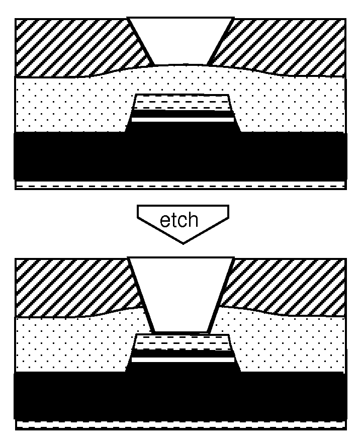
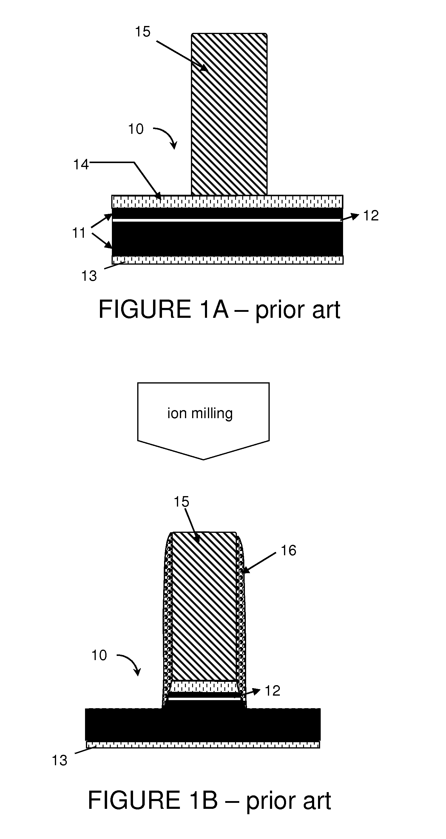
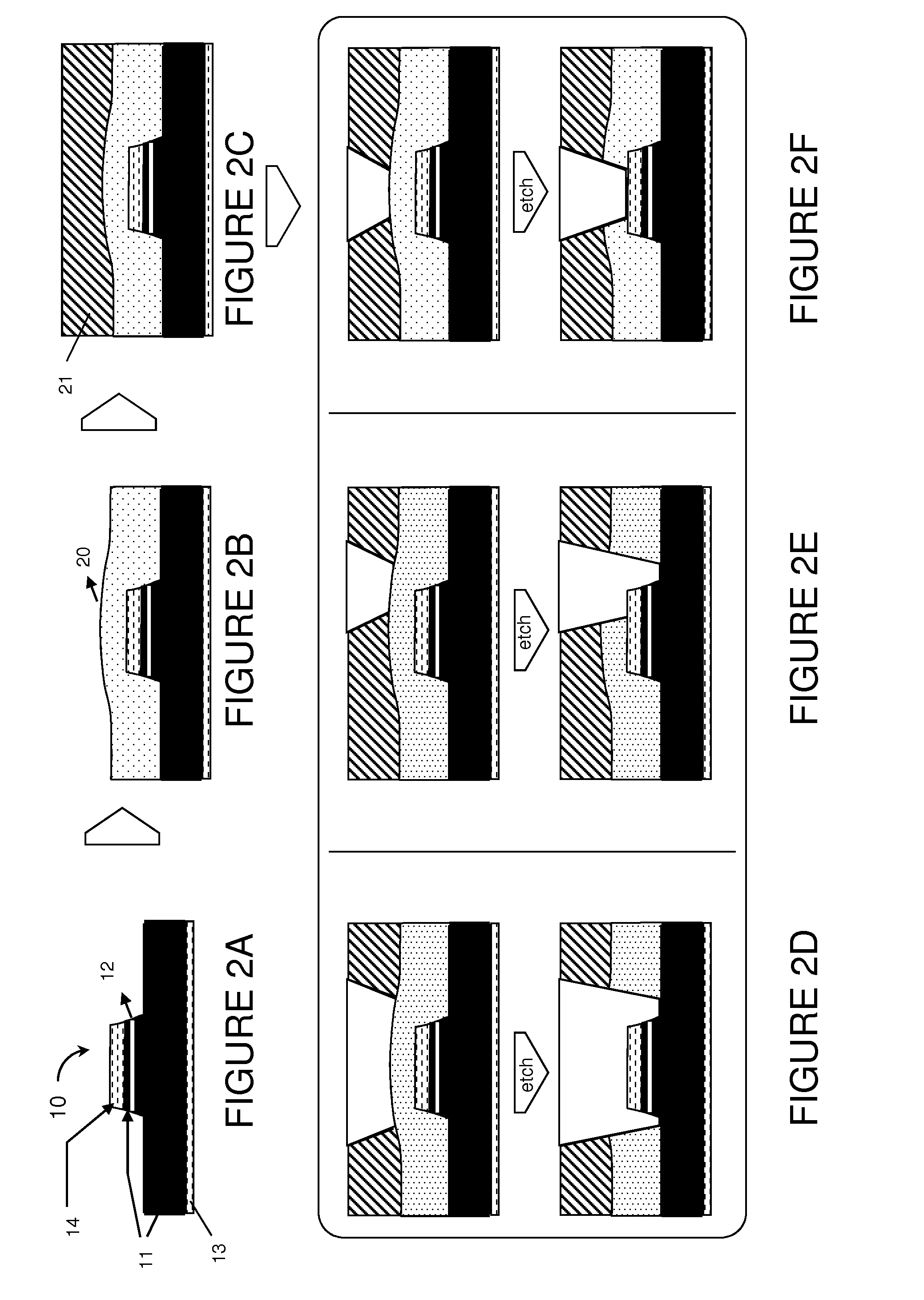
[0031]The present invention will be described with respect to particular embodiments and with reference to certain drawings but the invention is not limited thereto but only by the claims. The drawings described are only schematic and are non-limiting. In the drawings, the size of some of the elements may be exaggerated and not drawn on scale for illustrative purposes. The dimensions and the relative dimensions do not correspond to actual reductions to practice of the invention.

[0032]Moreover, the term top and the like in the description and the claims are used for descriptive purposes and not necessarily for describing relative positions. It is to be understood that the terms so used are interchangeable under appropriate circumstances and that the illustrative embodiments described herein are capable of operation in other orientations than described or illustrated herein.

[0033]It is to be noticed that the term “comprising”, used in the claims, should not be interpreted as being res...


PUM

PropertyMeasurementUnit
Thicknessaaaaaaaaaa
Thicknessaaaaaaaaaa
Heightaaaaaaaaaa

Abstract

A method according to embodiments of the present invention comprises providing a magnetic stack comprising a magnetic layer sub-stack comprising magnetic layers and a bottom conductive electrode and a top conductive electrode electrically connecting the magnetic layer sub-stack at opposite sides thereof; providing a sacrificial pillar on top of the magnetic stack, the sacrificial pillar having an undercut with respect to an overlying second sacrificial material and a sloped foot with increasing cross-sectional dimension towards the magnetic stack, using the sacrificial pillar for patterning the magnetic stack, depositing an insulating layer around the sacrificial pillar, selectively removing the sacrificial pillar, thus creating a contact hole towards the patterned magnetic stack, and filling the contact hole with electrically conductive material.

Description

FIELD OF THE INVENTION[0001]The present invention relates to the field of patterning of magnetic layers. Furthermore, the present invention relates to the fabrication of magnetic devices.BACKGROUND OF THE INVENTION[0002]Nowadays, the use of magnetic layers for micro- and nano-devices gains lots of interest for many applications, such as for example MRAM memories, spin torque oscillators, hard disk read heads and sensor applications, and even magnetic logic circuits. An important problem occurring during processing of such devices is the patterning of the magnetic layers. Magnetic devices typically comprise multilayers of ultrathin magnetic and non-magnetic layers. Reactive etching of such multilayers is difficult, because of the variation in materials, which requires different etchants for different materials. Therefore, the patterning of such multilayer stacks is done typically using Reactive Ion Etching (RIE) or ion milling techniques. A drawback of these techniques is the redepos...

Claims


Application Information

Patent Timeline
IPC IPC(8): B32B3/00C23F1/04H01F41/34B05D3/00B05D3/10B05D5/12B05D5/00
CPCY10T428/24802H01L43/12Y10T29/49043Y10T29/49046Y10T29/49048H10N50/01
Inventor OP DE BEECK, MARIALAGAE, LIESBET
Owner INTERUNIVERSITAIR MICRO ELECTRONICS CENT (IMEC VZW)
Why Eureka
Try Eureka