Carrier bonding and detaching processes for a semiconductor wafer

a technology of carrier bonding and detachment, which is applied in the direction of transportation and packaging, containers, paper/cardboard containers, etc., can solve problems such as damage to the wafer, and achieve the effect of easy detachmen

Inactive Publication Date: 2012-03-01
ADVANCED SEMICON ENG INC
View PDF3 Cites 32 Cited by
  • Summary
  • Abstract
  • Description
  • Claims
  • Application Information

AI Technical Summary

Benefits of technology

[0008]Another aspect of the disclosure relates to a method for handling a semiconductor wafer. In one embodiment, the method comprises attaching a first carrier to an active surface of the semiconductor wafer using a first adhesive, wherein a first isolation layer is disposed between the first adhesive and the first carrier. The method can further include the step of attaching a second car

Problems solved by technology

However, this process can damage the wafer particu

Method used


Image

  • Carrier bonding and detaching processes for a semiconductor wafer
  • Carrier bonding and detaching processes for a semiconductor wafer
  • Carrier bonding and detaching processes for a semiconductor wafer

Examples


Embodiment Construction

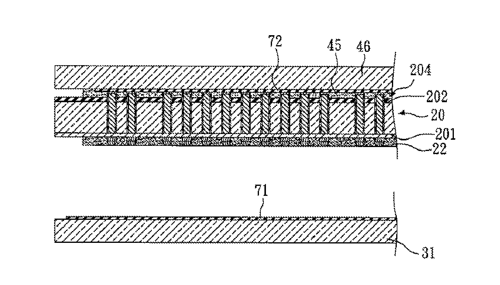
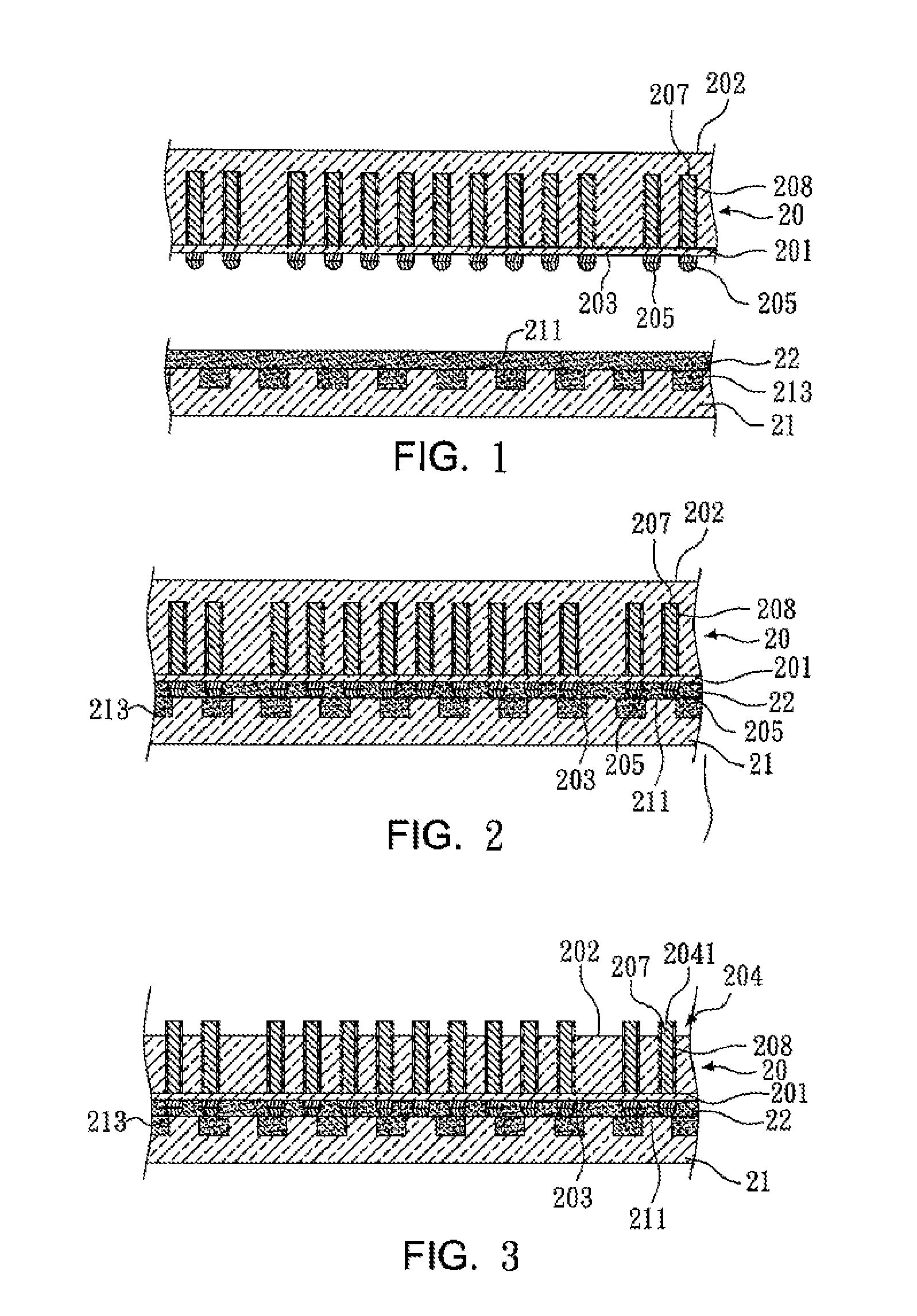
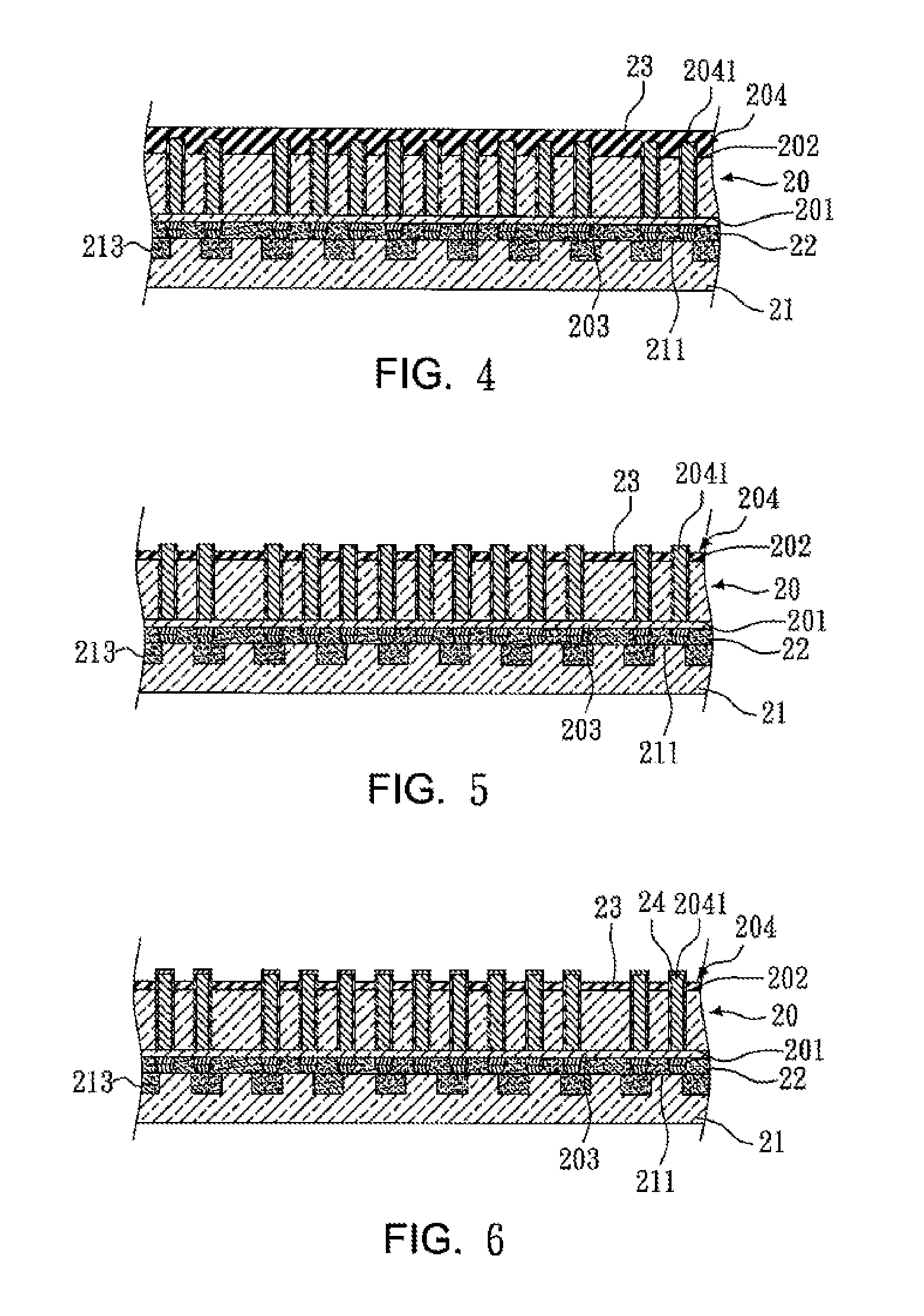
[0018]Referring to FIG. 1, a semiconductor wafer 20 (shown in a cross-sectional view) being prepared for handling and transportation, according to an embodiment of the present invention is illustrated. The semiconductor wafer 20 has a first surface 201, a second surface 202 and a plurality of conductive pillars 207. The semiconductor wafer 20 can be made from silicon, germanium, gallium arsenide, etc. and the conductive pillars 207 made of a suitable conductive material such as copper. In this embodiment, the semiconductor wafer 20 can be fully fabricated to include an integrated circuit 203 and the conductive pillars 207 (as shown), or may be an interposer having only the conductive pillars 207. To avoid placing conductive metal directly on the semiconductor material, an insulation material 208, such as a non-conductive polymer, including polyimide (PI), epoxy or benzocyclobutene (BCB), or an inorganic material, such as, silicon dioxide (SiO2), is formed between the semiconductor m...


PUM

PropertyMeasurementUnit
Temperatureaaaaaaaaaa
Electrical conductoraaaaaaaaaa
Transparencyaaaaaaaaaa

Abstract

The present invention provides a temporary carrier bonding and detaching process. A first surface of a semiconductor wafer is mounted on a first carrier by a first adhesive layer, and a first isolation coating disposed between the first adhesive layer and the first carrier. Then, a second carrier is mounted on the second surface of the semiconductor wafer. The first carrier is detached. Then, the first surface of the semiconductor wafer is mounted on a film frame. The second carrier is detached. The method of the present invention utilizes the second carrier to support and protect the semiconductor wafer, after which the first carrier is detached. Therefore, the semiconductor wafer will not be damaged or broken, thereby improving the yield rate of the semiconductor process. Furthermore, the simplicity of the detaching method for the first carrier allows for improvement in efficiency of the semiconductor process.

Description

CROSS-REFERENCE TO RELATED APPLICATIONS[0001]This application claims the benefit of Taiwan application Serial No. 099128960, filed 27 Aug. 2010, the subject matter of which is incorporated herein by reference.BACKGROUND OF THE INVENTION[0002]1. Field of the Invention[0003]The present invention relates generally to semiconductor device manufacturing, and more particularly, to handling and transport of semiconductor wafers during manufacturing.[0004]2. Description of the Related Art[0005]Handling semiconductor wafers that are in an intermediate state of fabrication as they are transported from one manufacturing site to another requires extreme care such that damage to the wafers is prevented. Conventionally, wafer chucks are mounted on surfaces of the wafer or carrier. However, this process can damage the wafer particularly when the chucks are detached from the wafer. As efforts to reduce the thickness of semiconductor wafers continue, improved techniques for their handling and transp...

Claims


Application Information

Patent Timeline
IPC IPC(8): H01L21/302B32B37/02H01L21/677B32B37/12
CPCH01L21/486H01L21/6835H01L21/6836Y10T156/10H01L2221/6834H01L2221/68381H01L2221/68327H01L21/76898
Inventor YANG, KUO-PINHSIAO, WEI-MINHUNG, CHENG-HUI
Owner ADVANCED SEMICON ENG INC
Why Eureka
Try Eureka