LED package structure and packaging method thereof

a technology of light-emitting diodes and package structures, applied in the direction of semiconductor/solid-state device manufacturing, electrical equipment, semiconductor devices, etc., can solve the problems of shortening the wavelength of light beam, affecting the characteristics and use life of led chips, and affecting the reliability of components, etc., to achieve the effect of increasing the reliability of components

Inactive Publication Date: 2012-03-08
DELTA ELECTRONICS INC
View PDF2 Cites 17 Cited by
  • Summary
  • Abstract
  • Description
  • Claims
  • Application Information

AI Technical Summary

Benefits of technology

[0008]The present invention provides a LED package structure and a process of manufacturing the LED package structure by wireless interconnection, thereby increasing the component reliability and avoiding the problem of causing insufficient adhesion and wire damage of the conventional wire bonding process.

Problems solved by technology

However, in a case that the LED package structure is operated at high power, the heat-dissipating efficacy may affect the characteristics and the use life of the LED chip.
If the heat accumulated within the LED package structure fails to be dissipated away, an elevated temperature at the contacts may impair the illuminating efficiency, shorten the wavelength of the light beam and reduce the use life.
In the SMD-LED package structure, since the thermal conductivity of the encapsulant member is relatively low, it is difficult to dissipate away the heat that is within the package structure.
The heat accumulation may deteriorate the performance, use life and reliability of the LED package structure.
Moreover, since the difference between the thermal conductivities of the LED chip and the encapsulant member is very obvious, the stability and use life of the LED package structure are adversely affected.
Once the SMD-LED package structure is soldered within a high-temperature oven at a temperature of 250° C.˜300° C., some defects may be generated in the SMD-LED package structure.
However, since the adhesion of the wire to the substrate electrode is possibly insufficient or the wire is possibly broken, the reliability of the conventional LED package structure is impaired.

Method used


Image

  • LED package structure and packaging method thereof
  • LED package structure and packaging method thereof
  • LED package structure and packaging method thereof

Examples


first embodiment

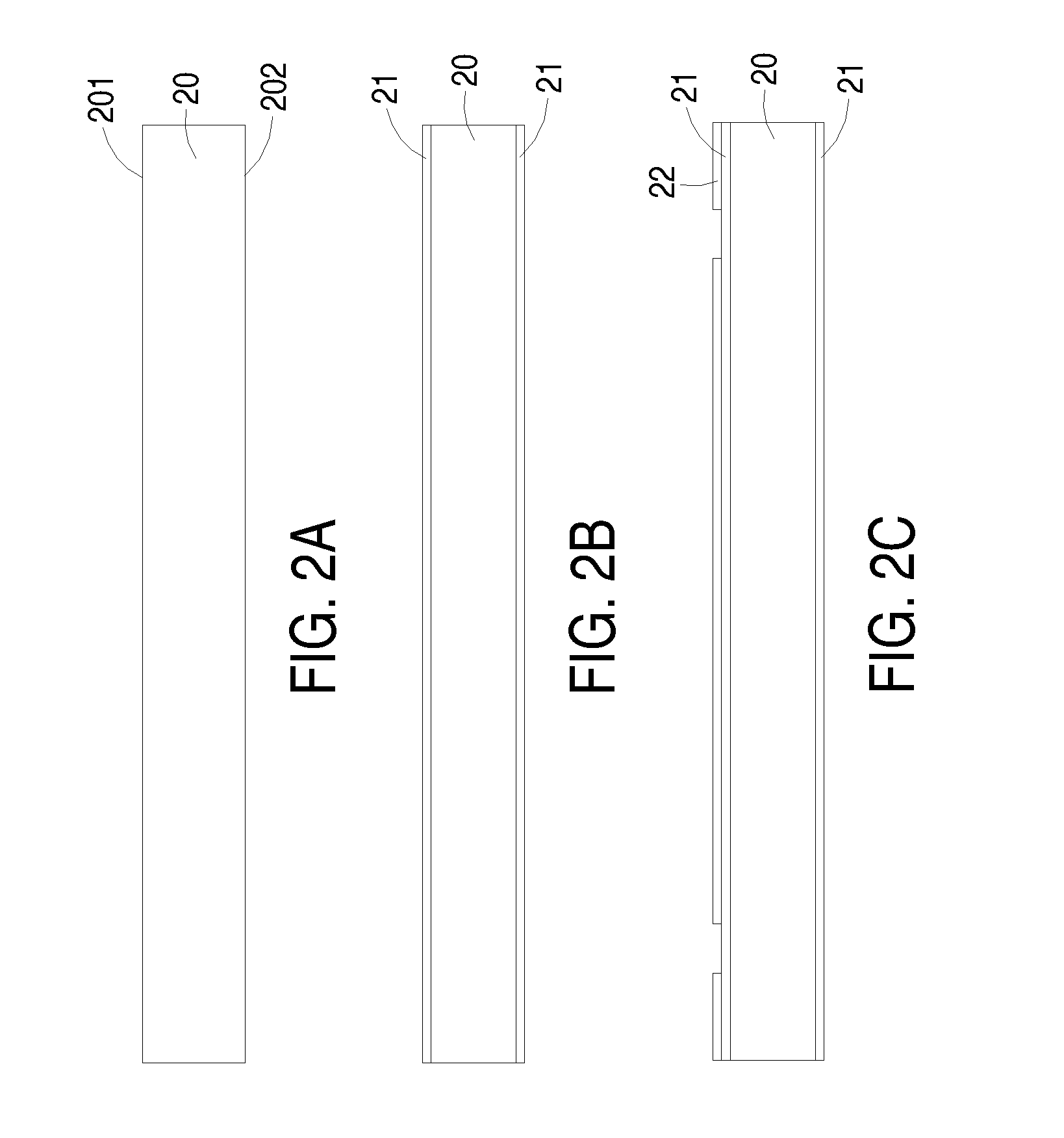
[0025]FIGS. 2A˜2S schematically illustrate a method of manufacturing a LED package structure according to the present invention. Firstly, as shown in FIG. 2A, a supporting substrate 20 includes a top surface 201 and a bottom surface 202. The supporting substrate 20 is, for example, a silicon wafer. After a heat treatment is performed, the silicon dioxide layers are formed on the top surface 201 and the bottom surface 202 of the silicon wafer to serve as the etching stop layers 21 (see FIG. 2B). In comparison with the conventional metallic lead frame, the surface of the silicon wafer is smoother and suitable for performing a eutectic bonding process. Moreover, the silicon wafer has some additional benefits such as high thermal conductivity, high melting point and low mechanical stress. In addition, the thermal expansion coefficient of the silicon wafer is similar to that of the optoelectronic semiconductor.

[0026]The supporting substrate 20 is not limited to the silicon wafer. In some...

second embodiment

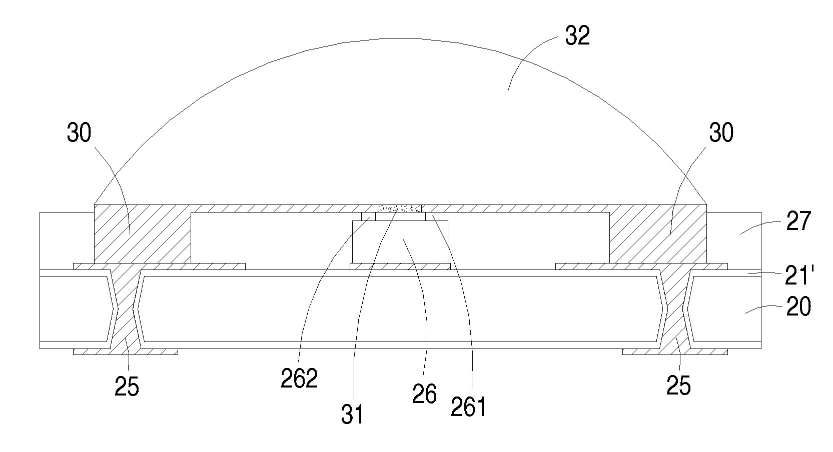
[0046]FIGS. 7A˜7S schematically illustrate a method of manufacturing a LED package structure according to the present invention. The configuration of the resulting LED package structure is shown in FIG. 7S. Except that the supporting substrate 20 further comprises a concave structure 33 (see FIG. 7E) and the LED chip 26 is accommodated and fixed within the concave structure 33 (see FIG. 7M), the steps of manufacturing the LED package structure of FIG. 7S are similar to those of FIG. 2, and are not redundantly described herein. Moreover, the first electrically-conductive structure 25 is selectively formed on a portion of the surface of the concave structure 33 (see FIG. 7L), or only formed in the first channel 24 and the supporting substrate 20 between the first channel 24 and the concave structure 33.

[0047]From the above discussion, the LED package structure of the second embodiment includes a supporting substrate 20, a first electrically-conductive structure 25, a LED chip 26, an i...

third embodiment

[0051]FIGS. 8A˜8G schematically illustrate a method of manufacturing a LED package structure according to the present invention. The configuration of the resulting LED package structure is shown in FIG. 8G. Similar to FIG. 7K, a supporting substrate 20 having a concave structure 33 and a first channel 24 is shown in FIG. 8A. The way of forming the concave structure 33 and the first channel 24 are similar to those illustrated in FIGS. 7A˜7J, and are not redundantly described herein. In this embodiment, the concave structure 33 is relatively deeper for accommodating the whole LED chip 26 in the sequent steps.

[0052]Then, as shown in FIG. 8B, a first electrically-conductive structure 25 is formed on the surface of the first channel 24 and partially formed on the top surface 201 and the bottom surface 202 of the supporting substrate 20, and a metallic base layer 251 for sequent die-bonding process is formed on the bottom surface of the concave structure 33. The first electrically-conduct...


PUM


Abstract

A LED package structure includes a supporting substrate, a first electrically-conductive structure, a LED chip, an insulating layer and a second electrically-conductive structure. The supporting substrate includes a top surface, a bottom surface and a first channel. The first electrically-conductive structure is filled in the first channel and partially formed on the top and bottom surfaces of the supporting substrate. The LED chip is disposed over the supporting substrate. The insulating layer is formed over the supporting substrate and on bilateral sides of the LED chip. The insulating layer has a second channel corresponding to the first electrically-conductive structure. The second electrically-conductive structure is filled in the second channel and partially formed on the insulating layer, and connected with an electrode of the LED chip. The LED chip and the top and bottom surfaces of the supporting substrate are connected with each other through the first and second electrically-conductive structures.

Description

FIELD OF THE INVENTION[0001]The present invention relates to a light emitting diode package structure and packaging method, and more particularly to a light emitting diode package structure and packaging method by employing a wireless interconnection technology.BACKGROUND OF THE INVENTION[0002]Generally, a LED chip is packaged into a LED package structure in order to assure electrical connection between the LED chip and the substrate and protect the LED chip from damage by foreign attack (e.g. mechanical shock, heat or moisture). Depending on applications, shapes, heat-dissipating mechanisms and illuminating mechanisms, the LED package structures are classified into several types such as Lamp-LED, TOP-LED, Side-LED, SMD-LED, High-Power-LED, Flip Chip-LED, and the like.[0003]Hereinafter, a process of manufacturing a SMD-LED (surface mount LED) package structure will be illustrated in more details. Firstly, a LED chip is fixed on a small substrate. Then, the LED chip is electrically c...

Claims


Application Information

Patent Timeline
Patent Type & Authority Applications(United States)
IPC IPC(8): H01L33/50H01L33/48H01L33/62
CPCH01L24/24H01L33/50H01L2924/12041H01L2924/3025H01L2924/10253H01L2224/45144H01L2224/45124H01L2924/014H01L2924/01322H01L2924/01047H01L2924/01033H01L2924/01019H01L2924/01006H01L33/54H01L33/60H01L33/62H01L2224/48091H01L2224/48227H01L2924/01013H01L2924/01079H01L2924/01082H01L2933/0066H01L2924/00014H01L2924/00H01L2224/73267H01L2924/15153H01L2924/15787H01L2924/15788
Inventor HSIEH, HSIEH-SHENCHEN, CHAO-MINLIN, LI-FANCHEN, SHIH-PENGCHEN, HUANG-KUN
Owner DELTA ELECTRONICS INC
Why Eureka
Try Eureka