Cmos-inverter-type frequency divider circuit, and mobile phone including the cmos-inverter-type frequency divider circuit
a frequency divider circuit and inverter-type technology, applied in the field of cmos-inverter-type frequency divider circuits, can solve the problems of wasteful power consumption, unnecessary large current flow, and low power consumption of such frequency divider circuits, so as to eliminate the design margin, further reduce power consumption, and reduce power consumption.
- Summary
- Abstract
- Description
- Claims
- Application Information
AI Technical Summary
Benefits of technology
Problems solved by technology
Method used
Image
Examples
first embodiment
[0035]
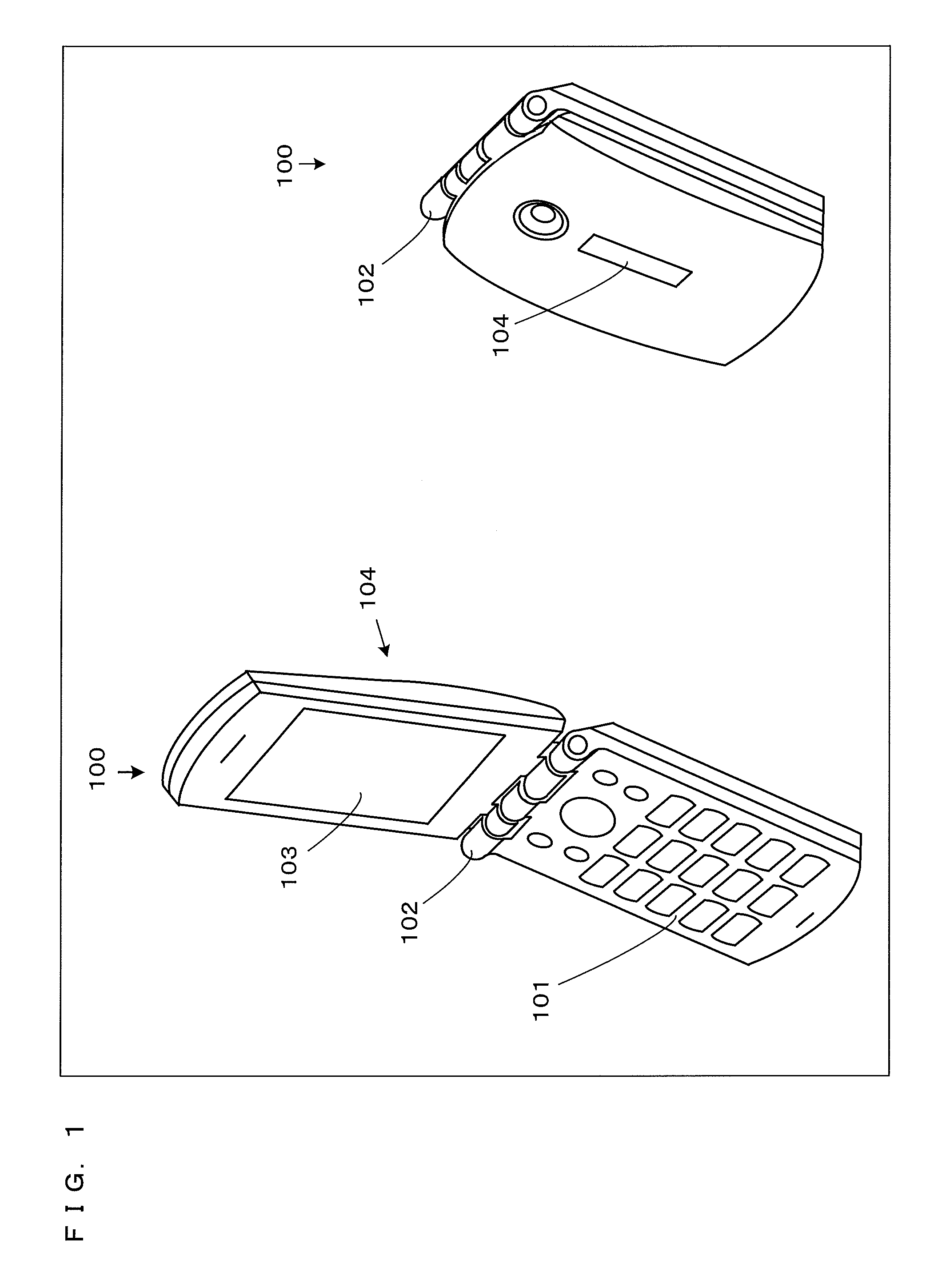
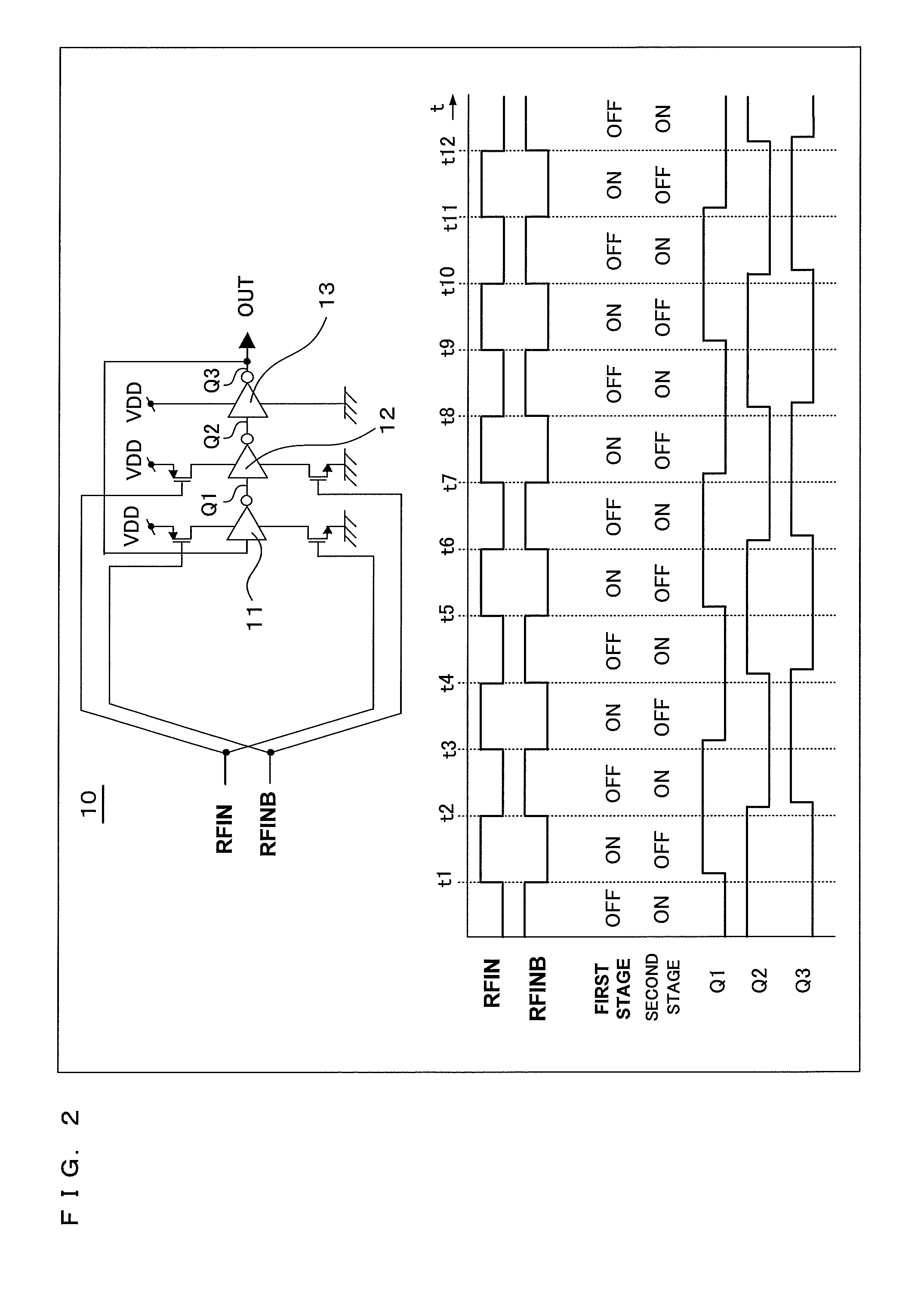
[0036]A CMOS-inverter-type frequency divider circuit according to the present embodiment is used for a transmitter of a mobile phone or the like, and supplies as much power as needed depending on time, to each CMOS inverter, thereby realizing reduction of power consumption. More specifically, an input indicating whether the VCO sub band selection or normal transmission is performed is received, whereby the amount of power to be supplied for driving each CMOS inverter is switched between the VCO sub band selection and the normal transmission. Here, particularly, in the normal transmission, the individual differences are corrected based on a threshold value of a dummy MOS transistor, and the gate voltage of a MOS transistor provided in series on a power line of each CMOS inverter is adjusted such that the free-running frequency of each CMOS inverter is smaller than the maximum frequency that can be used in the VCO sub band selection, and is not smaller than the maximum frequency...
second embodiment
[0068]
[0069]As in the first embodiment, a CMOS-inverter-type frequency divider circuit according to the present embodiment is used for a transmitter of a mobile phone or the like, and supplies as much power as needed depending on time, to each CMOS inverter, thereby realizing reduction of power consumption. In the first embodiment, the gate voltage of the MOS transistor provided in series on the power line of each CMOS inverter is adjusted, whereby the current consumption is restricted. On the other hand, in the present embodiment, the supply voltage for each CMOS inverter is restricted, whereby the power consumption is reduced.
[0070]
[0071]FIG. 5 is a schematic diagram showing a divide-by-2 frequency divider circuit 50 of clocked inverter type according to the present embodiment.
[0072]It is noted that the same components as those in the first embodiment are denoted by the same reference numerals.
[0073]As shown in FIG. 5, in addition to the components of the divide-by-2 frequency div...
PUM
 Abstract
Description
Claims
Application Information


