Distributed cooling of arrayed semi-conductor radiation emitting devices

Inactive Publication Date: 2012-03-15
PRESSCO IP LLC
View PDF24 Cites 12 Cited by
  • Summary
  • Abstract
  • Description
  • Claims
  • Application Information

AI Technical Summary

Benefits of technology

[0006]In one aspect of the presently described embodiments, the system comprises a mounting substrate to which the array of semi-conductor based radiation emitting devices is mounted on a first surface thereof, the mounting substrate including at least one of a first material having high thermal conductivity and a second material having

Problems solved by technology

Indeed, the primary failure mode of any semi-conductor devices is the damage that can occur during overheating.
Metal heat sinks and forced air systems have the disadvantage of low cooling capacity, with the best possible

Method used


Image

  • Distributed cooling of arrayed semi-conductor radiation emitting devices
  • Distributed cooling of arrayed semi-conductor radiation emitting devices
  • Distributed cooling of arrayed semi-conductor radiation emitting devices

Examples


Embodiment Construction

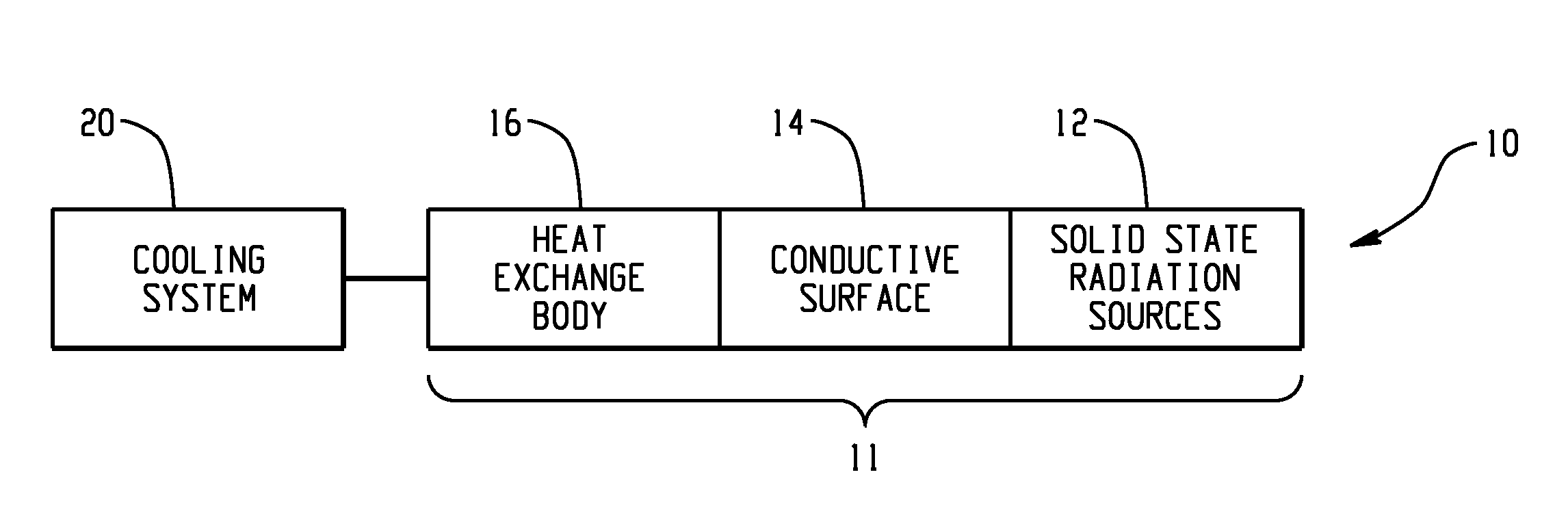
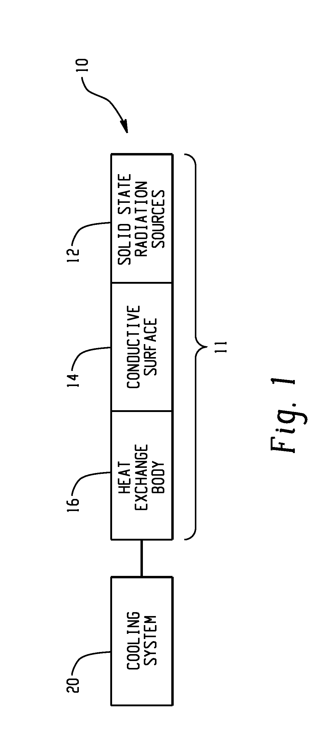
[0039]A purpose of the presently described embodiments is to apply a properly sized cooling system to solid state, semi-conductor based electromagnetic irradiation device arrays used in heating and curing applications. One such application involves systems for cooking food. Another application of the presently described embodiments is to systems using narrowband semi-conductor based radiant heating of plastic components, such as PET bottle preforms in a bottle blowing process.

[0040]The contemplated cooling system may take a variety of forms including heat transfer fluid systems such as state change cooling systems (including vapor phase (or two phase) cooling systems), water based cooling systems (including systems using water mixtures including, e.g. ethylene glycol), air cooling systems or common refrigerant cooling systems (e.g. systems using chlorofluorocarbons (CFCs), hydro chlorofluorocarbons (HCFCs), butane, or propane).

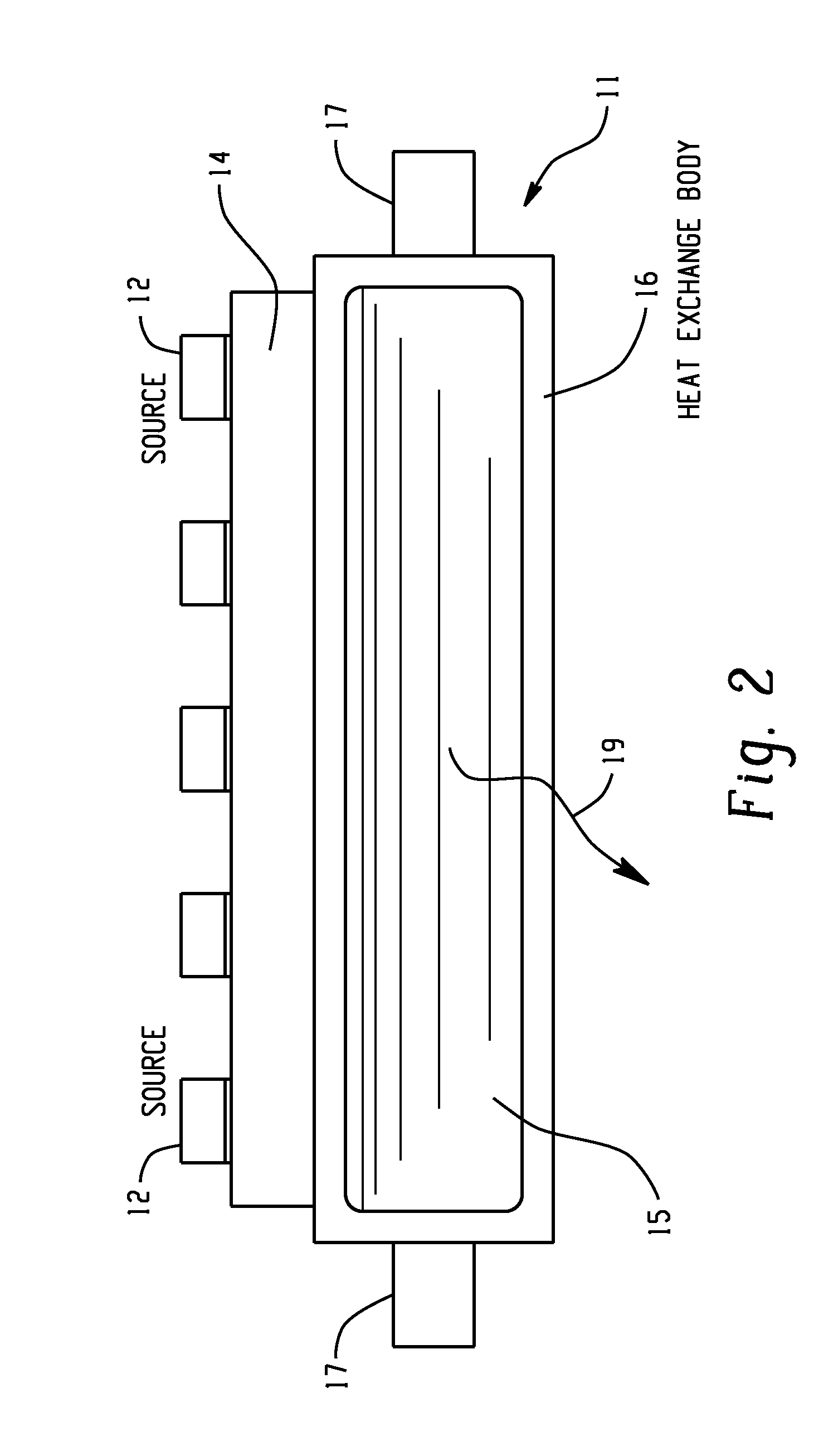
[0041]With reference to FIG. 1, a system 10 includes sol...


PUM


Abstract

Techniques for the removal of waste heat from solid state, semiconductor devices (such as cooking or heating devices) are provided. In particular, techniques for conducting waste heat away from the device through a heat sink in contact with a cooling system are provided. In addition, a multi-head cooling system applicable to multiple solid state, semiconductor sources is provided.

Description

[0001]This application is based on and claims priority to U.S. Provisional Application No. 61 / 350,352, filed Jun. 1, 2010, which is incorporated herein by reference in its entirety.FIELD[0002]The presently described embodiments relate, in general, to a novel system configuration(s) and associated methods for the removal of waste heat from solid state, semi-conductor array cooking systems and, in particular, to the conduction of the waste heat away from the devices array through a heat sink in contact with a cooling system. In addition, this application includes a design of a multi-head cooling system applicable to cool multiple solid state, semi-conductor array irradiation sources.BACKGROUND[0003]The advantages of heating and cooking with irradiation produced by arrays of semi-conductor devices have been well documented. For example, a prior patent, U.S. Pat. No. 7,425,296, discloses such advantages. Increased device lifetime, greater output energy control, improved energy efficienc...

Claims


Application Information

Patent Timeline
IPC IPC(8): F28F7/00
CPCF21V29/006F21V29/02F21V29/402F21V29/30H05B6/642H05B2214/04F21Y2101/02F21Y2115/10
Inventor KATZ, JONATHAN M.JOHNSON, BENJAMIN D.
Owner PRESSCO IP LLC
Why Eureka
Try Eureka