
Radio frequency integrated circuit for enhanced transmit/receive performance in low power applications and method of making the same

Inactive Publication Date: 2012-03-15
US SEC THE ARMY THE
View PDF9 Cites 9 Cited by
  • Summary
  • Abstract
  • Description
  • Claims
  • Application Information

AI Technical Summary

Benefits of technology

[0009]The embodiments of the invention provide a simplified design with the goal of being able to work with / enhance the RFIC's from multiple vendors. Moreover, a significant objective of the described preferred embodiments is to minimize the amount of software or other changes on the part of a given vendor; essentially a “drop in” technology (i.e., insertable into an existing system) geared towards optimizing the performance of existing RFIC's for use in high noise or extended range applications.
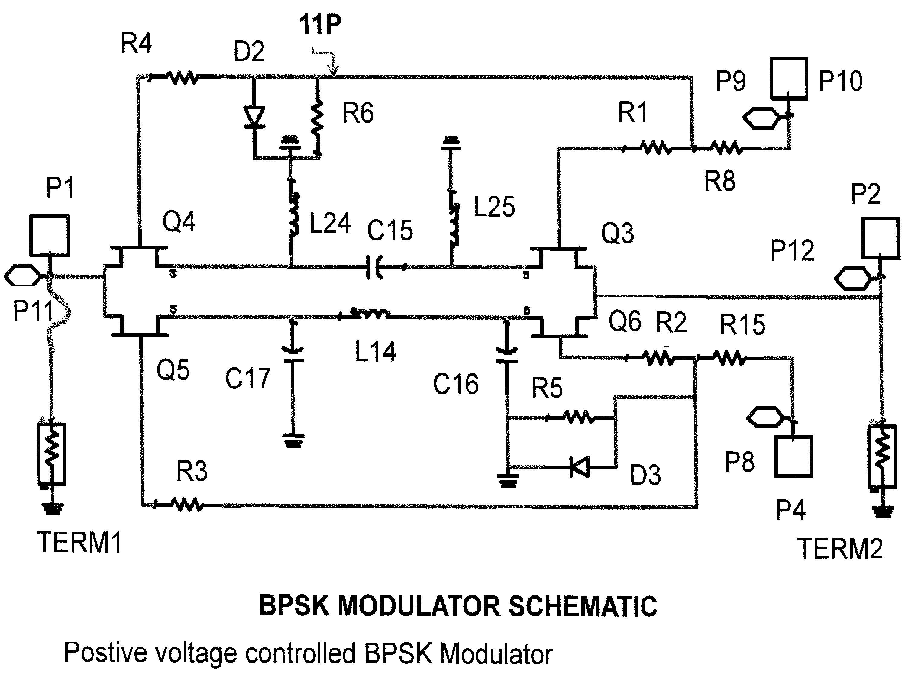
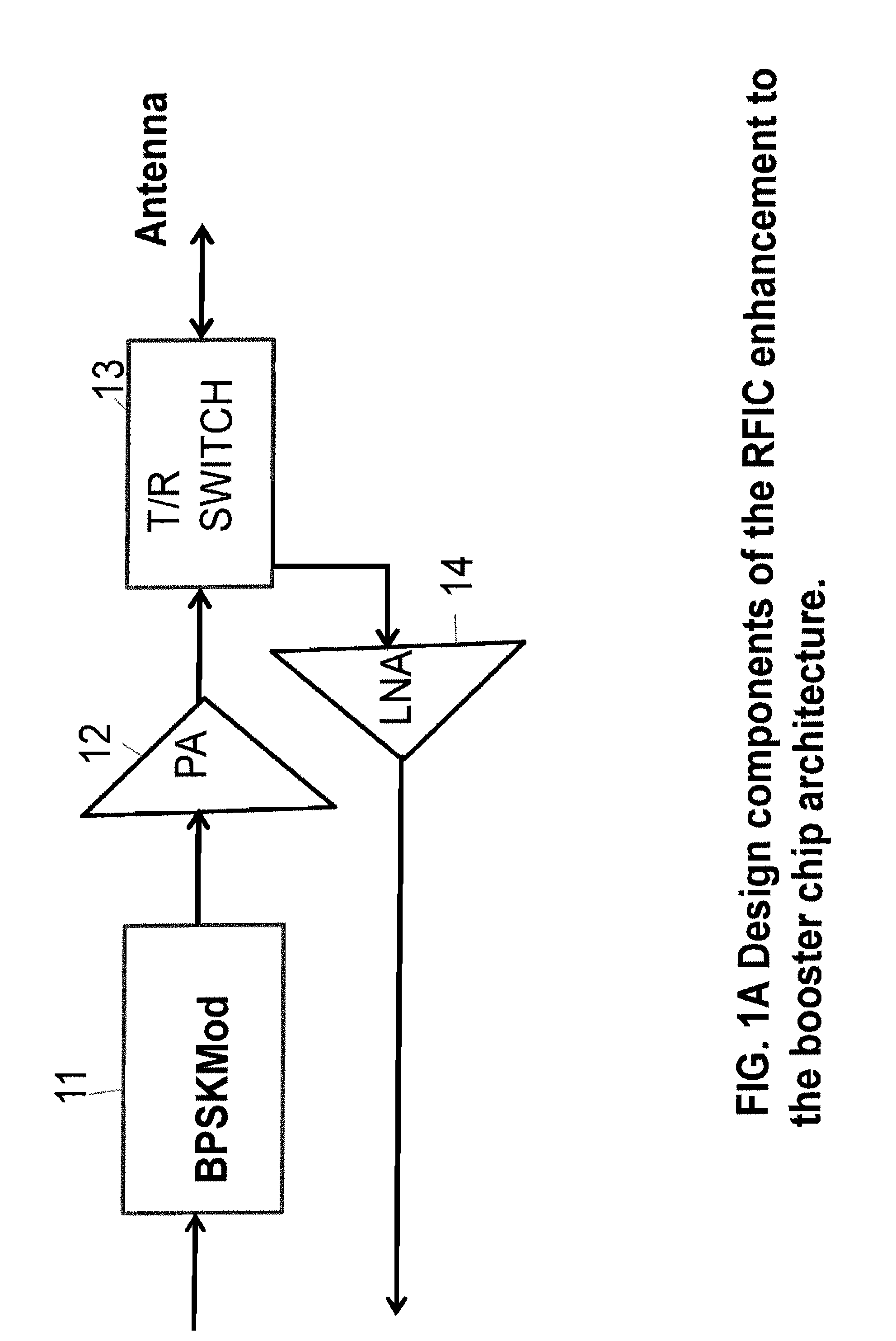
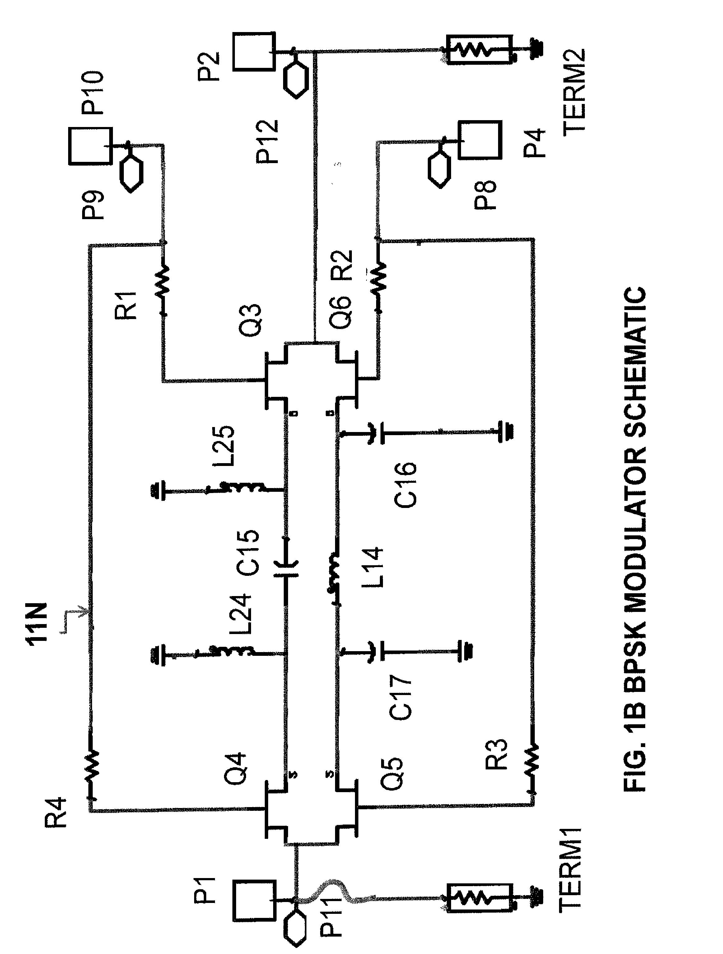
[0010]The invention can be used to enhance the performance of wireless RF systems using commercial parts. It could also be used as a standalone binary phase shift keying (BPSK) modulation system by adding the digital controller and an oscillator source using the RFIC booster chip as the front end of a transceiver.
[0011]Military and commercial applications using wireless data transmission are numerous and constantly growing in new directions. In low-power military applications, a tradeoff between transmit range and battery life exists. A simple means of extending transmit range would be to add the described custom integrated circuit (IC) between the transceiver and antenna. By way of example, the invention could be used to enhance the use of unattended ground sensor systems; allowing for the retrieval of sensor data from greater distances.
[0013]A block diagram representation of a preferred embodiment booster chip is depicted in FIG. 1. FIG. 8 depicts an RFIC narrowband 450-MHz booster chip on a 4×4 mm tile to enhance performance of a companion integrated circuit (IC) on a GaAs substrate. The transmit stage of the circuit consists of the BPSK modulator cascaded with a power amplifier and TR switch. The receive stage of the circuit consists of the TR switch cascaded with the LNA. The BPSK modulator is a novel component and typically exists off-chip. There are additional gate enable DC inputs to provide a higher level of isolation between the power amplifier and LNA stages than is currently available. These gate enable features are also novel to this invention and are denoted in FIG. 7 as “LNAen” and “PAen”, respectively. This will save power consumption and provide additional isolation between transmit and receive stages. This isolation could be essential for system level performance, and provides an additional 60 dB of isolation between transmit and receive beyond the 35-40 dB of isolation provided by the TR switch. This additional isolation could be provided in the other designs by providing switching supplies for the separate LNA and power amplifier supply inputs, but this would require significant board area compared to the simple gate enable inputs. The BPSK modulator has a negative DC OFF state of approximately 3.0 V and an ON state of 0.0 V to activate the A and B control pins. The TR switch has a positive DC reference of 2.5 V on the control inputs corresponding to ON and 0.0 V corresponding to OFF, which activate the transmit stage or the receive stage, respectively. The PA and LNA both have a +2.7 to +3.0 V supply voltage.

Problems solved by technology

The simulations show that the gains and input matches of both stages usually fall within desired ranges; however, the LNAs often have a poor input match in order to minimize the NF.

Method used


Image

  • Radio frequency integrated circuit for enhanced transmit/receive performance in low power applications and method of making the same
  • Radio frequency integrated circuit for enhanced transmit/receive performance in low power applications and method of making the same
  • Radio frequency integrated circuit for enhanced transmit/receive performance in low power applications and method of making the same

Examples


Embodiment Construction

[0091]The embodiments of the invention and the various features and advantageous details thereof are explained more fully with reference to the non-limiting embodiments that are illustrated in the accompanying drawings and detailed in the following description. It should be noted that the features illustrated in the drawings are not necessarily drawn to scale. Descriptions of well-known components and processing techniques are omitted so as to not unnecessarily obscure the embodiments of the invention. The examples used herein are intended merely to facilitate an understanding of ways in which the embodiments of the invention may be practiced and to further enable those of skill in the art to practice the embodiments of the invention. Accordingly, the examples should not be construed as limiting the scope of the embodiments of the invention. Rather, these embodiments are provided so that this disclosure will be thorough and complete, and will fully convey the scope of the invention ...


PUM

PropertyMeasurementUnit
Electric potential / voltageaaaaaaaaaa

Abstract

A radio frequency integrated circuit (and method of making) for enhancing wireless communication and / or sensing systems comprising a base comprising a gallium arsenide (GaAs) substrate; a binary phase shift keying modulator fabricated on the base; a power amplifier fabricated on the base and operatively associated with the binary phase shift keying modulator; the power amplifier having a first shunt operatively associated therewith; a transmit / receive switch fabricated on the base, the transmit / receive switch being operatively associated with the power amplifier and being alternately connectable to an antenna port adapted to be connected to an antenna; a low noise amplifier fabricated on the base; the low noise amplifier being alternately connectable to the antenna port, the low noise amplifier having a second shunt operatively associated therewith; the circuit operating in a transmit stage in which the power amplifier is connected to the antenna port and in a receive stage in which the low noise amplifier is connected to the antenna port; whereby in the receive stage the power amplifier is bypassed by the first shunt to reduce current consumption and substantially isolate the receive stage from the transmit stage; and in the transmit stage the low noise amplifier is bypassed by the second shunt to reduce current consumption and to substantially isolate the transmit stage from the receive stage.

Description

STATEMENT OF GOVERNMENT INTEREST[0001]The invention described herein may be manufactured, used, and licensed by or for the United States Government.FIELD OF THE INVENTION[0002]This invention relates broadly to IC circuits and in particular to radio frequency integrated circuits.BACKGROUND OF THE INVENTION / DESCRIPTION OF THE RELATED ART[0003]High performance microwave and radio frequency integrated circuits are of interest both for military and civilian applications. The ability to design custom integrated circuits and fabricate prototypes in a timely and cost effective manner is a prime concern. Low-power sensor networks have recently become very popular for applications such as logistics and home automations. Remote low-power radio frequency (RF) applications are becoming more prevalent and low power tends to mean short transmission range. This necessitates the need to develop custom RF enhancement chips to meet military and commercial needs that can't be met by commercial off the ...

Claims


Application Information

Patent Timeline
IPC IPC(8): H04L27/20H05K3/10
CPCY10T29/49155H04B1/40
Inventor PENN, JOHN E.MITCHELL, GREGORY A.
Owner US SEC THE ARMY THE
Learn More