Semiconductor device

Active Publication Date: 2012-03-15
SEMICON ENERGY LAB CO LTD
View PDF2 Cites 20 Cited by
  • Summary
  • Abstract
  • Description
  • Claims
  • Application Information

AI Technical Summary

Benefits of technology

[0012]In view of the above problems, an object of an embodiment of the present invention is to provide a semiconductor device with a novel

Problems solved by technology

Moreover, since leakage current (off-state current) flows between a source and a drain of a transistor included in a storage element when the transistor is in an off state for example, electric charge flows into or out even if the transistor is not selected, which makes a data holding period short.
For that reason, another writing operation (refresh operation) is necessary at predetermined intervals, and it is difficult to sufficiently reduce power consumption.
Furthermore, since stored data is lost when power is not supplied, an additional storage device using a magnetic material or an optical material is needed in order to hold data for a long time.
However, cost per storage capacity is increased because a circuit such

Method used


Image

  • Semiconductor device
  • Semiconductor device
  • Semiconductor device

Examples


embodiment 1

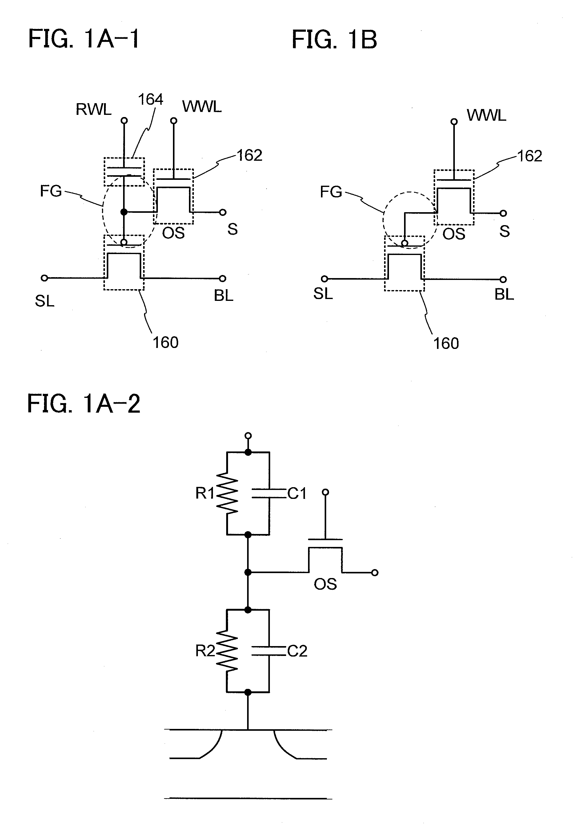
[0053]In this embodiment, a circuit structure and operation of a semiconductor device according to an embodiment of the disclosed invention will be described with reference to FIGS. 1A-1 to 1B and FIGS. 2A to 2C. Note that in each of the circuit diagrams, in some cases, “OS” is written beside a transistor in order to indicate that the transistor includes an oxide semiconductor.

[0054]First, the most basic circuit structure of a memory cell and its operation will be described with reference to FIGS. 1A-1 to 1B. In a semiconductor device including a memory cell illustrated in FIG. 1A-1, a bit line BL and a source electrode (or a drain electrode) of a transistor 160 are electrically connected to each other, and a source line SL and the drain electrode (or the source electrode) of the transistor 160 are electrically connected to each other. In addition, a signal line S and a source electrode (or a drain electrode) of a transistor 162 are electrically connected to each other, and a write ...

application example

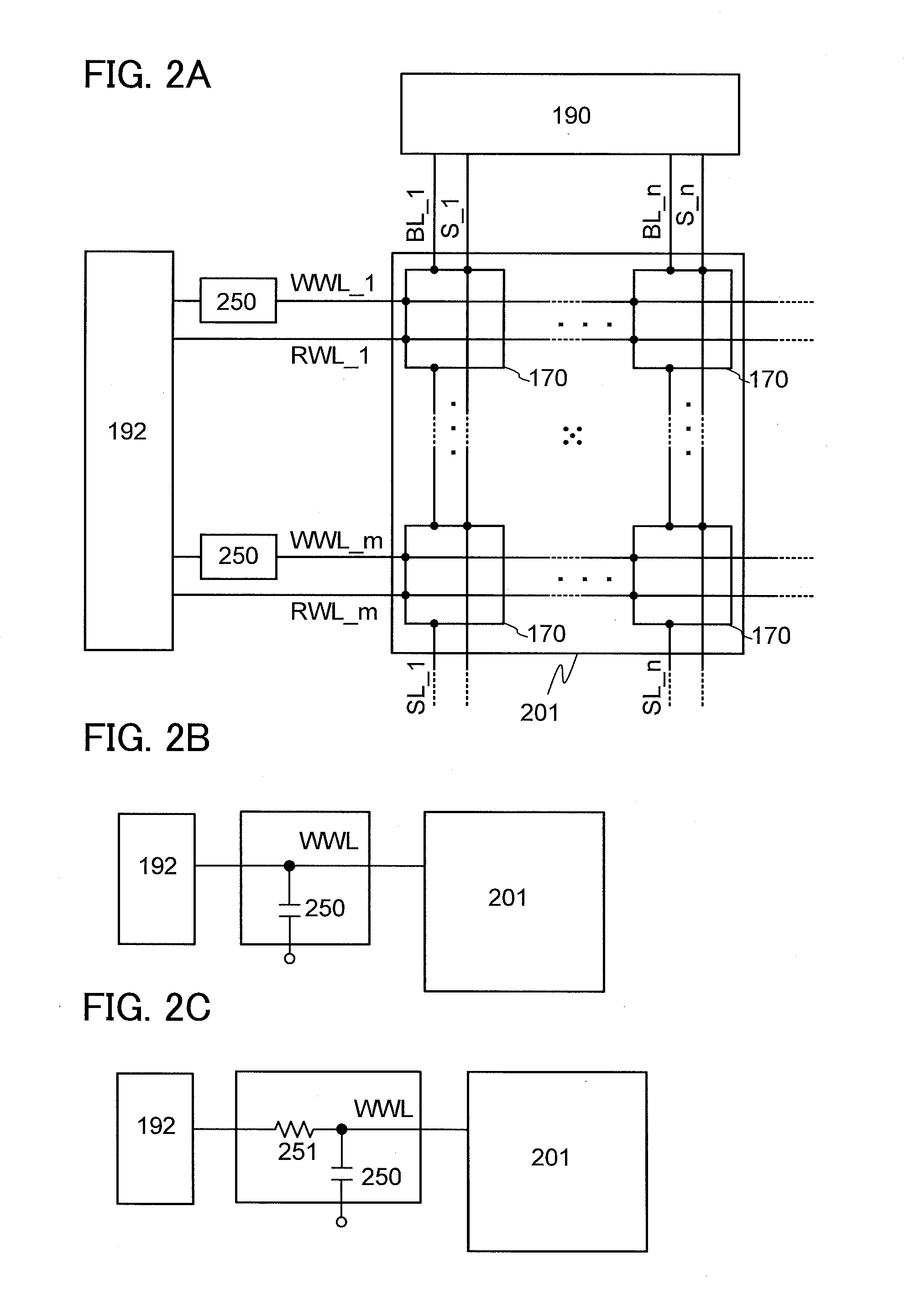
[0083]Next, a more specific circuit structure to which the circuit of the memory cell illustrated in FIGS. 1A-1 to 1B is applied and an operation thereof will be described with reference to FIGS. 2A to 2C.

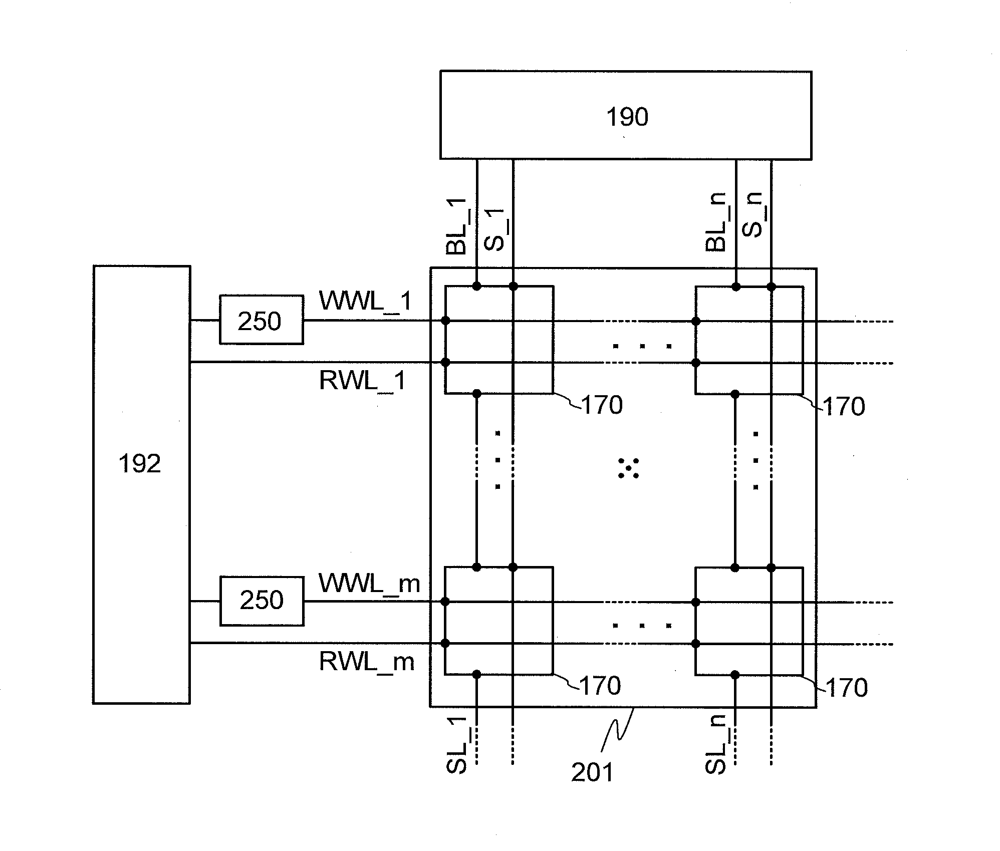
[0084]FIG. 2A is an example of a circuit diagram of a semiconductor device including (m×n) memory cells 170. The structure of the memory cells 170 in FIG. 2A is similar to that in FIG. 1A-1. Note that in FIG. 2A, only the memory cells 170 in the first row are directly connected to the bit lines BL, and only the memory cells 170 in the m-th row are directly connected to the source lines SL. The memory cells 170 in other rows are electrically connected to the bit lines BL and the source lines SL through other memory cells 170 in the same columns.

[0085]The semiconductor device in FIG. 2A includes m (m is an integer of greater than or equal to 2) write word lines WWL, in read word lines RWL, n (n is an integer of greater than or equal to 2) source lines SL, n bit lines BL, n signal lin...

embodiment 2

[0105]In this embodiment, a circuit structure to which the circuit of the memory cell illustrated in FIGS. 1A-1 to 1B is applied and which is different from that in FIGS. 2A to 2C will be described with reference to FIGS. 3A to 3D and FIGS. 4A to 4F.

[0106]FIG. 3A is an example of a circuit diagram of a semiconductor device including (m×n) memory cells 170. The structure of the memory cells 170 in FIG. 3A is similar to that in FIG. 1A-1 and FIG. 2A; therefore, the detailed description thereof is omitted.

[0107]The semiconductor device in FIG. 3A includes a memory cell array 201 including the memory cells 170 arranged in a matrix of m (rows)×n (columns), a first driver circuit 190 connected to n bit lines BL and n signal lines S, and a second driver circuit 192 connected to m write word lines WWL and in read word lines RWL.

[0108]In the semiconductor device illustrated in FIG. 3A, the second driver circuit 192 includes a noise removal circuit 260 that is electrically connected to the wr...


PUM


Abstract

A semiconductor device in which stored data can be held even when power is not supplied and there is no limitation on the number of writing operations is provided. A semiconductor device is formed using a material which can sufficiently reduce the off-state current of a transistor, such as an oxide semiconductor material that is a wide-gap semiconductor. When a semiconductor material which can sufficiently reduce the off-state current of a transistor is used, the semiconductor device can hold data for a long period. In addition, by providing a capacitor or a noise removal circuit electrically connected to a write word line, a signal such as a short pulse or a noise input to a memory cell can be reduced or removed. Accordingly, a malfunction in which data written into the memory cell is erased when a transistor in the memory cell is instantaneously turned on can be prevented.

Description

BACKGROUND OF THE INVENTION[0001]1. Field of the Invention[0002]An embodiment of the present invention relates to a semiconductor device including a semiconductor element and a method for driving the semiconductor device.[0003]2. Description of the Related Art[0004]Storage devices including semiconductor elements are broadly classified into two categories: a volatile device that loses stored data when power is not supplied, and a non-volatile device that holds stored data even when power is not supplied.[0005]A typical example of a volatile storage device is a DRAM (dynamic random access memory). A DRAM stores data in such a manner that a transistor included in a storage element is selected and electric charge is stored in a capacitor.[0006]When data is read from a DRAM, electric charge in a capacitor is lost on the above-described principle; thus, another writing operation is necessary whenever data is read out. Moreover, since leakage current (off-state current) flows between a so...

Claims


Application Information

Patent Timeline
IPC IPC(8): G11C11/24
CPCG11C8/08G11C11/403G11C11/405G11C11/4085H01L27/1052G11C16/0433G11C16/0483G11C16/08G11C2211/4016G11C16/02H01L27/1214H10B99/00
Inventor MATSUZAKI, TAKANORINAGATSUKA, SHUHEIINOUE, HIROKI
Owner SEMICON ENERGY LAB CO LTD
Why Eureka
Try Eureka