Photovoltaic device with a zinc magnesium oxide window layer

a photovoltaic and window layer technology, applied in the field of semiconductor devices, can solve the problems of large loss in voc and

Active Publication Date: 2012-03-22
JPMORGAN CHASE BANK NA
View PDF6 Cites 13 Cited by
  • Summary
  • Abstract
  • Description
  • Claims
  • Application Information

AI Technical Summary

Problems solved by technology

Theoretical modeling has shown that a more negative Δ leads to larger loss in Voc and FF

Method used


Image

  • Photovoltaic device with a zinc magnesium oxide window layer
  • Photovoltaic device with a zinc magnesium oxide window layer
  • Photovoltaic device with a zinc magnesium oxide window layer

Examples


Embodiment Construction

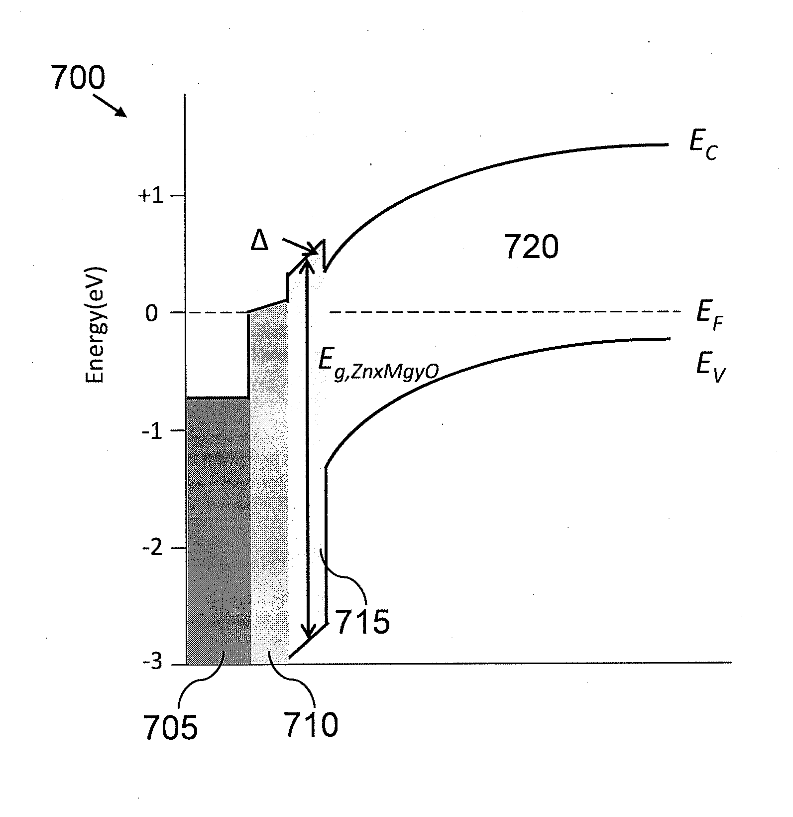
[0018]This disclosure is directed to photovoltaic devices and methods of production. In one embodiment, Zn1−xMgxO is employed for a window layer of substrate structure. FIG. 3 depicts substrate structure 300 according to one embodiment. Substrate structure 300 includes substrate 305, transparent conductive oxide (TCO) layer 310, buffer layer 315 and window layer 320. TCO layer 310 may typically be employed to allow solar radiation to enter a photovoltaic device and may further act as an electrode. TCO layer 310 may include an n-type material doped with one of SnO2 and Cd2SnO4. Window layer 320 may be employed to mitigate the internal loss of photo carriers (e.g., electrons and holes) in the device and may strongly influence device parameters including open circuit voltage (Voc), short circuit current (Isc) and fill factor (FF). In one embodiment, window layer 320 may allow incident light to pass to an absorber material to absorb light. According to one embodiment, to improve overall...


PUM


Abstract

Methods and devices are described for a photovoltaic device and substrate structure. In one embodiment, a photovoltaic device includes a substrate structure and a CdTe absorber layer, the substrate structure including a Zn1−xMgxO window layer and a low conductivity buffer layer. Another embodiment is directed to a process for manufacturing a photovoltaic device including forming a Zn1−xMgxO window layer over a substrate by at least one of sputtering, evaporation deposition, CVD, chemical bath deposition process and vapor transport deposition process. The process including forming a CdTe absorber layer above the Zn1−xMgxO window layer.

Description

CROSS REFERENCE TO RELATED APPLICATION[0001]This application claims priority under 35 U.S.C. § 119(e) to Provisional Application No. 61 / 385,399 filed on Sep. 22, 2010, which is hereby incorporated by reference in its entirety.FIELD OF THE INVENTION[0002]Embodiments of the invention relate to semiconductor devices and methods of manufacture, and more particularly to the field of photovoltaic (PV) devices.BACKGROUND OF THE INVENTION[0003]Photovoltaic devices generally comprise multiple layers of material deposited on a substrate, such as glass. FIG. 1 depicts a typical photovoltaic device. Photovoltaic device 100 may employ a glass substrate 105, a transparent conductive oxide (TCO) layer 110 deposited on substrate 105, a window layer 115 made from an n-type semiconductor material, an absorber layer 120 made from a semiconductor material, and a metal back contact 125. Typical devices use cadmium telluride (CdTe) as absorber layer 120 and include glass substrate 105, tin oxide (SnO2) o...

Claims


Application Information

Patent Timeline
IPC IPC(8): H01L31/0264H01L31/18
CPCH01L31/022466Y02E10/543H01L31/1828H01L31/073H01L31/0224H01L31/022425H01L31/18H01L31/022483Y02P70/50H01L31/1884
Inventor SHAO, RUIGLOECKLER, MARKUS
Owner JPMORGAN CHASE BANK NA
Why Eureka
Try Eureka