Method for Vertical and Lateral Control of III-N Polarity

a technology of iiin and polarity, applied in the direction of basic electric elements, electrical apparatus, semiconductor devices, etc., can solve the problems of reducing the use of these materials, restricting the possible thickness, and affecting the film quality and resultant device performan

Active Publication Date: 2012-03-22
THE UNITED STATES OF AMERICA AS REPRESENTED BY THE SECRETARY OF THE NAVY
View PDF4 Cites 19 Cited by
  • Summary
  • Abstract
  • Description
  • Claims
  • Application Information

AI Technical Summary

Problems solved by technology

However, the requirement to use sapphire wafers reduces the use of these materials, as lattice and thermal mismatch between substrate and epitaxy introduce dislocations as well as restricting the possible thickness of the material.
This approach leads to ...

Method used


Image

  • Method for Vertical and Lateral Control of III-N Polarity
  • Method for Vertical and Lateral Control of III-N Polarity
  • Method for Vertical and Lateral Control of III-N Polarity

Examples


example 1

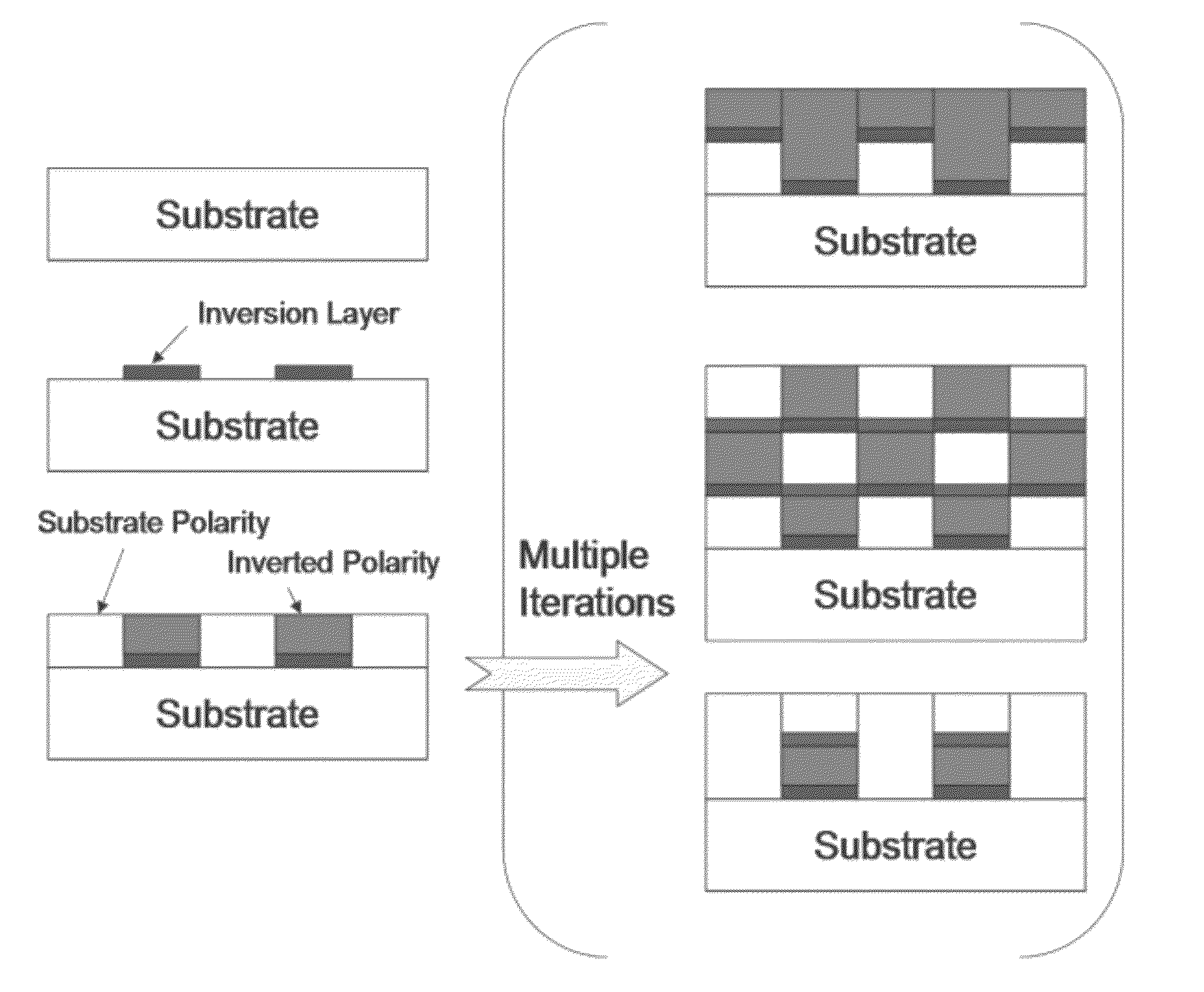
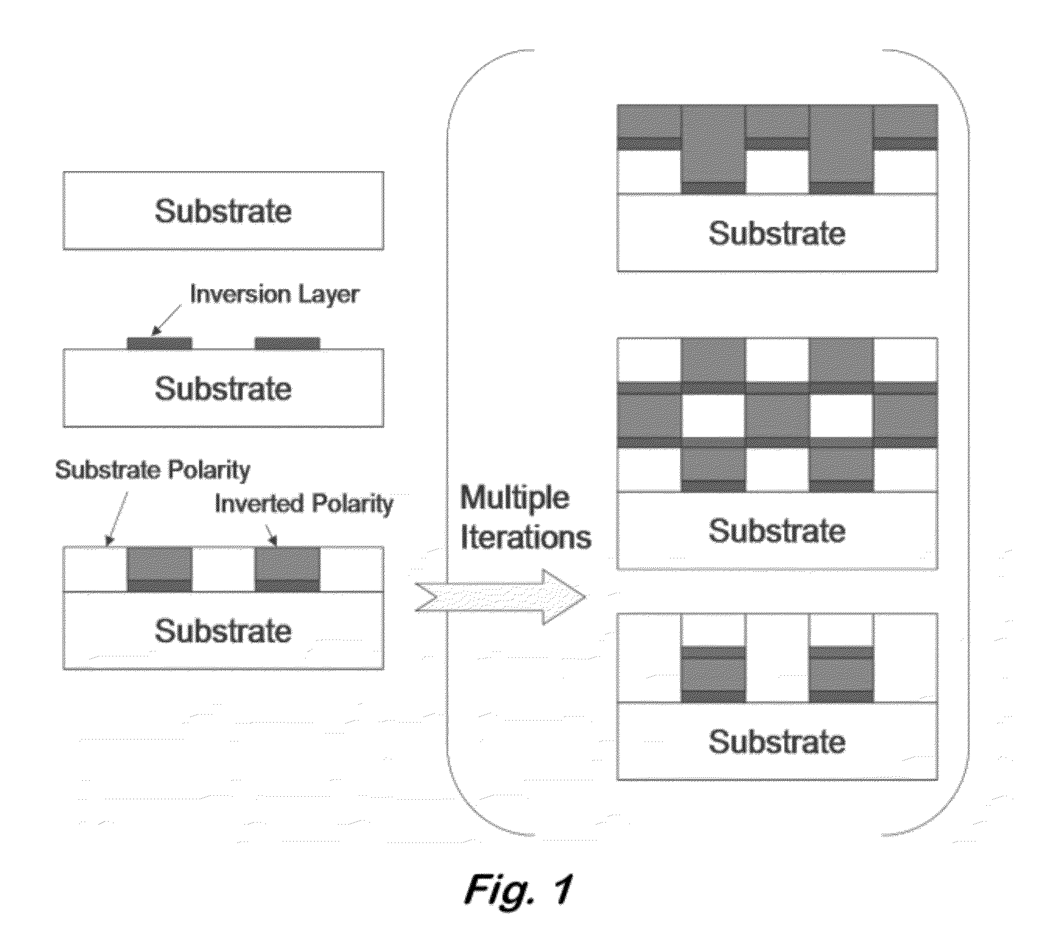
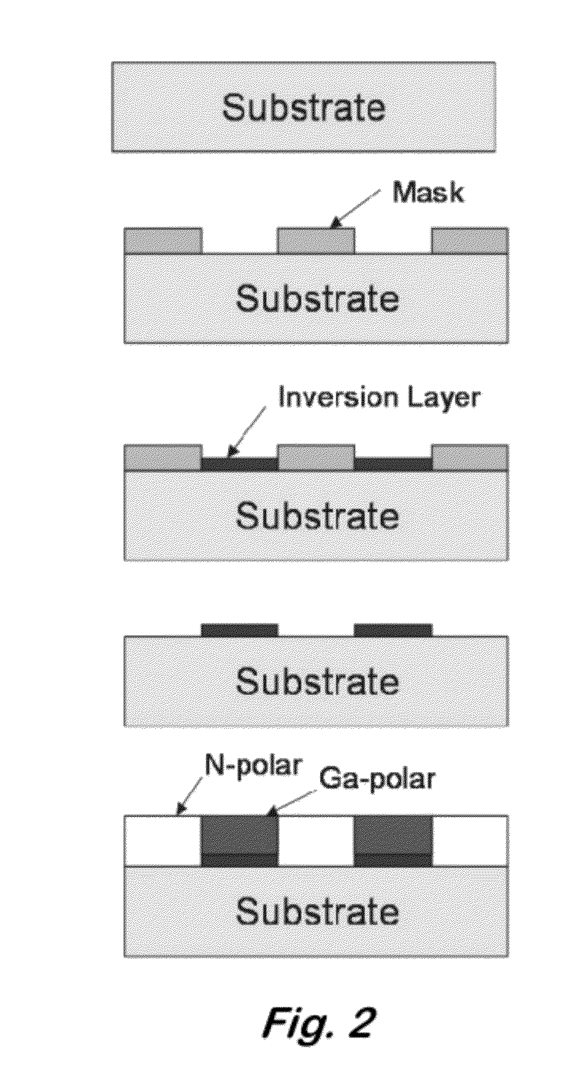
[0050]Sapphire substrate—The samples used in this study were grown in a Thomas Swan MOCVD vertical showerhead reactor. MOCVD-grown templates consisting of 1.5-2 μm thick epilayers of N-polar GaN on sapphire were used as substrates for a majority of this work, although several final samples were demonstrated on free-standing HVPE N-polar GaN substrates. A selective growth approach was taken to create the patterned inversion layer. In this case, the mask used consisted of stripes, but various geometries are possible. After patterning the substrate with standard photolithography steps, a SixNy layer was blanket deposited. Lift-off of the resist resulted in a SixNy masked pattern for confined epitaxial growth of the AlN inversion layer. This process has been previously developed and used in selective growth studies of III-N materials. The inversion layer was grown to a total thickness of 30 nm of AlN using trimethylaluminum and ammonia. Other conditions during this growth included a VII...

example 2

[0056]GaN substrate—The process was also employed on commercially available 1×1 cm2 HVPE N-polar GaN substrates. As the surfaces of these substrates have been CMP-polished, the issues with initial morphology in the form of hexagonal hillocks seen on samples on the MOCVD-grown N-polar templates should be eliminated. Indeed, SEM images of the lateral polarity structure on the HVPE sample (FIG. 9) resemble the images of lateral polarity structures grown directly on sapphire substrates (FIG. 5(a)). Although the surfaces of each polarity are still smooth, the interface between the two polarities is not as abrupt. In addition, for the N-polar regions, some regular faceting is seen. Both of these issues are believed to arise from misalignment between the mask and the substrate crystallographic direction. It may be possible to resolve this issue by improvements in lithographic procedures and better identification of crystallographic directions in the substrate crystal.

[0057]The slight diffe...

example 3

[0058]Templated substrate—A 2 μm thick MOCVD periodically patterned template was fabricated on a HVPE GaN substrate as described in Example 2. HVPE was used to extend the growth of the template to 50 μm thick. Cross-sectional SEM of the sample (FIG. 12) showed the MOCVD / HVPE interface to be sharp. Cross-sectional TEM of the sample (FIG. 13) shows the continuation of the alternating polarity in the template through the HVPE growth, as evidenced by the sharp inversion domain boundaries between the regions. TEM also shows a noticeable reduction in dislocation density in the Ga-polar regions with HVPE regrowth. This only improves with distance from the MOCVD / HVPE interface. By growing thick material, the difference in dislocation density between the two polar materials can be reduced. Photoluminescence mapping of the sample surface also show evidence of the regular spacing of inversion domain boundaries. This example demonstrates the use of HVPE to extend the alternating polarity materi...


PUM


Abstract

Disclosed herein is a method of: depositing a patterned mask layer on an N-polar GaN epitaxial layer of a sapphire, silicon, or silicon carbide substrate; depositing an AlN inversion layer on the open areas; removing any remaining mask; and depositing a III-N epitaxial layer to simultaneously produce N-polar material and III-polar material. Also disclosed herein is: depositing an AlN inversion layer on an N-polar bulk III-N substrate and depositing a III-N epitaxial layer to produce III-polar material. Also disclosed herein is: depositing an inversion layer on a III-polar bulk III-N substrate and depositing a III-N epitaxial layer to produce N-polar material. Also disclosed herein is a composition having: a bulk III-N substrate; an inversion layer on portions of the substrate; and a III-N epitaxial layer on the inversion layer. The III-N epitaxial layer is of the opposite polarity of the surface of the substrate.

Description

[0001]This application claims the benefit of U.S. Provisional Application No. 61 / 383,869, filed on Sep. 17, 2010. The provisional application and all other publications and patent documents referred to throughout this nonprovisional application are incorporated herein by reference.TECHNICAL FIELD[0002]The present disclosure is generally related to control of III-N polarity.DESCRIPTION OF RELATED ART[0003]Gallium nitride (GaN), a high performance semiconductor for both optical and electronic devices, can be grown in the c-direction of its lattice with two different polar faces, nitrogen- (N-) or gallium- (Ga-) polar. The face, or polar orientation, of the material establishes many of its properties, from chemical reactivity and dopant incorporation to spontaneous and piezoelectric-induced electric field directions in the crystal (Stutzmann et al., Phys. Status Solidi B 228 (2001) 505). Control of the polarization fields and, thus, polarization induced doping is the basis of Ga-polar ...

Claims


Application Information

Patent Timeline
IPC IPC(8): H01L29/20H01L21/20
CPCH01L21/0237H01L21/0242H01L21/02439H01L21/02639H01L21/02502H01L21/0254H01L21/02458H01L21/02378H01L21/02381H01L21/02389H01L21/02494H01L21/0262
Inventor HITE, JENNIFER K.KUB, FRANCIS J.EDDY, JR., CHARLES R.GARCES, NELSON
Owner THE UNITED STATES OF AMERICA AS REPRESENTED BY THE SECRETARY OF THE NAVY
Why Eureka
Try Eureka