Liquid crystal display device and method for manufacturing the same

a display device and liquid crystal technology, applied in semiconductor devices, instruments, optics, etc., can solve the problems of limiting the operation speed and geometric design rules of tft, easy operation method of touch screen, and enlarge the field of applications in a short time, so as to reduce the number of masks, facilitate the effect of reducing manufacturing cost and reducing light leakage curren

Active Publication Date: 2012-03-22
LG DISPLAY CO LTD
View PDF7 Cites 31 Cited by
  • Summary
  • Abstract
  • Description
  • Claims
  • Application Information

AI Technical Summary

Benefits of technology

[0023]An aspect of the present disclosure is to provide an LCD device, which facilitates lower manufacturing cost by reducing the number of masks for a process of forming a lower substrate, and a method for manufacturing the same.
[0024]Another aspect of the present disclosure is to provide a thin film transistor structure, which decreases a light leakage current in an active layer of a top gate structure, and a method for manufacturing the same.
[0025]Another aspect of the present disclosure is to provide an LCD device, which enhances manufacturing efficiency by simplifying a manufacturing process of a lower substrate, and a method for manufacturing the same.
[0026]Another aspect of the present disclosure is to provide an LCD device, which enhances driving performance by using LTPS (Low Temperature Poly Silicon) as the active semiconductor in the TFT.

Problems solved by technology

Furthermore, the easy operational method of the touch screen rapidly enlarges the field for applications.
Crosstalk is an undesirable visual phenomenon resulting from unintended pixels turning on to image misinformation.
The electron mobility property of amorphous silicon limits the operational speed and the geometric design rules of the TFT.
Therefore, the price competitiveness is limited and manufacturing efficiency is reduced.

Method used


Image

  • Liquid crystal display device and method for manufacturing the same
  • Liquid crystal display device and method for manufacturing the same
  • Liquid crystal display device and method for manufacturing the same

Examples


Embodiment Construction

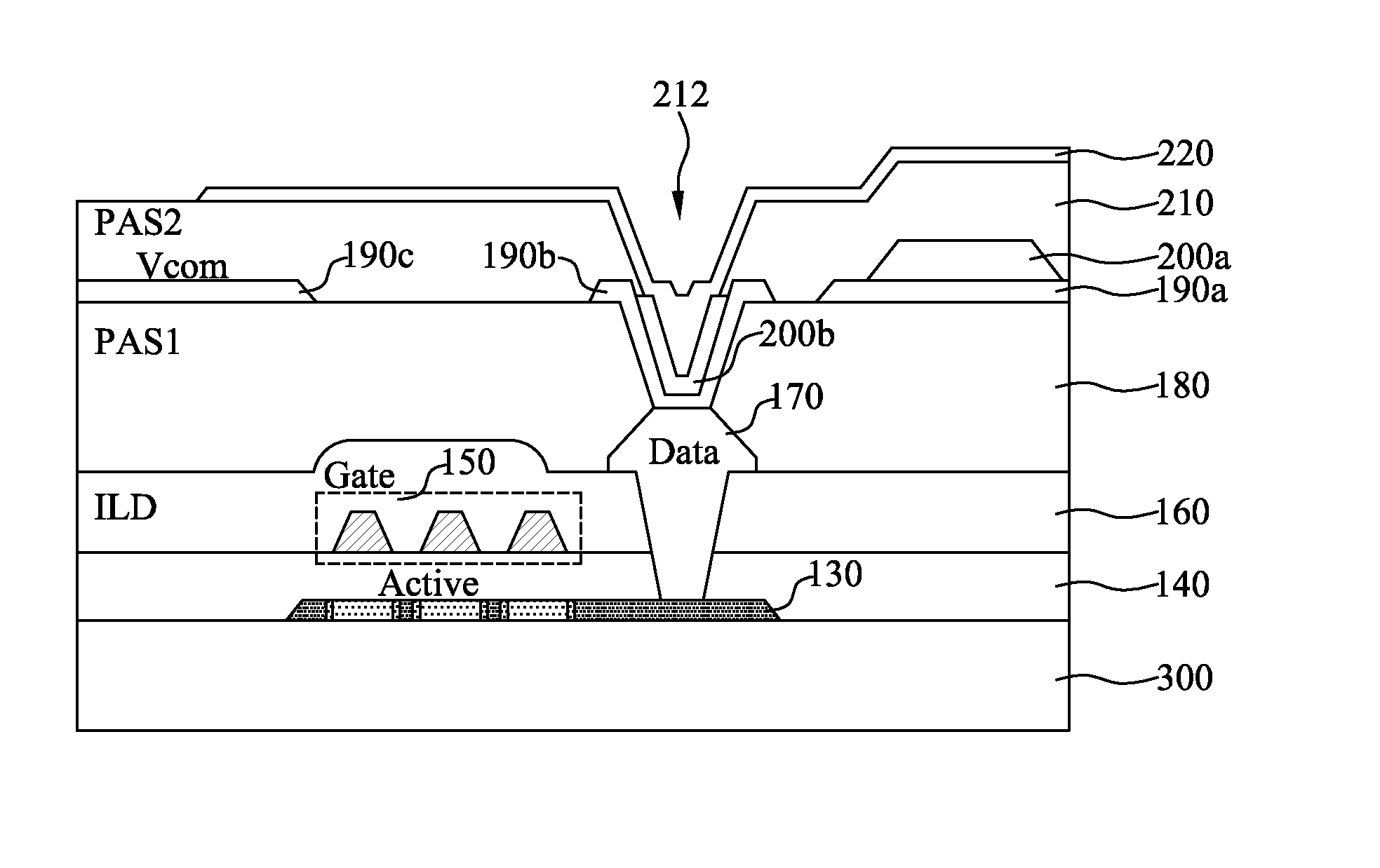
[0043]Reference will now be made in detail to the exemplary embodiments of the present disclosure, examples of which are illustrated in the accompanying drawings. Wherever possible, the same reference numbers will be used throughout the drawings to refer to the same or like parts.

[0044]Hereinafter, an LCD device with a built-in touch screen according to the present disclosure and a method for manufacturing the same will be described with reference to the accompanying drawings.

[0045]For the following description of the embodiments of the present disclosure, if a first structure (for example, electrode, line, layer, contact, and etc.) is described as being formed “on” or “under” a second structure, the first and second structures may come in contact with each other, or there may be a third structure interposed between the first and second structures.

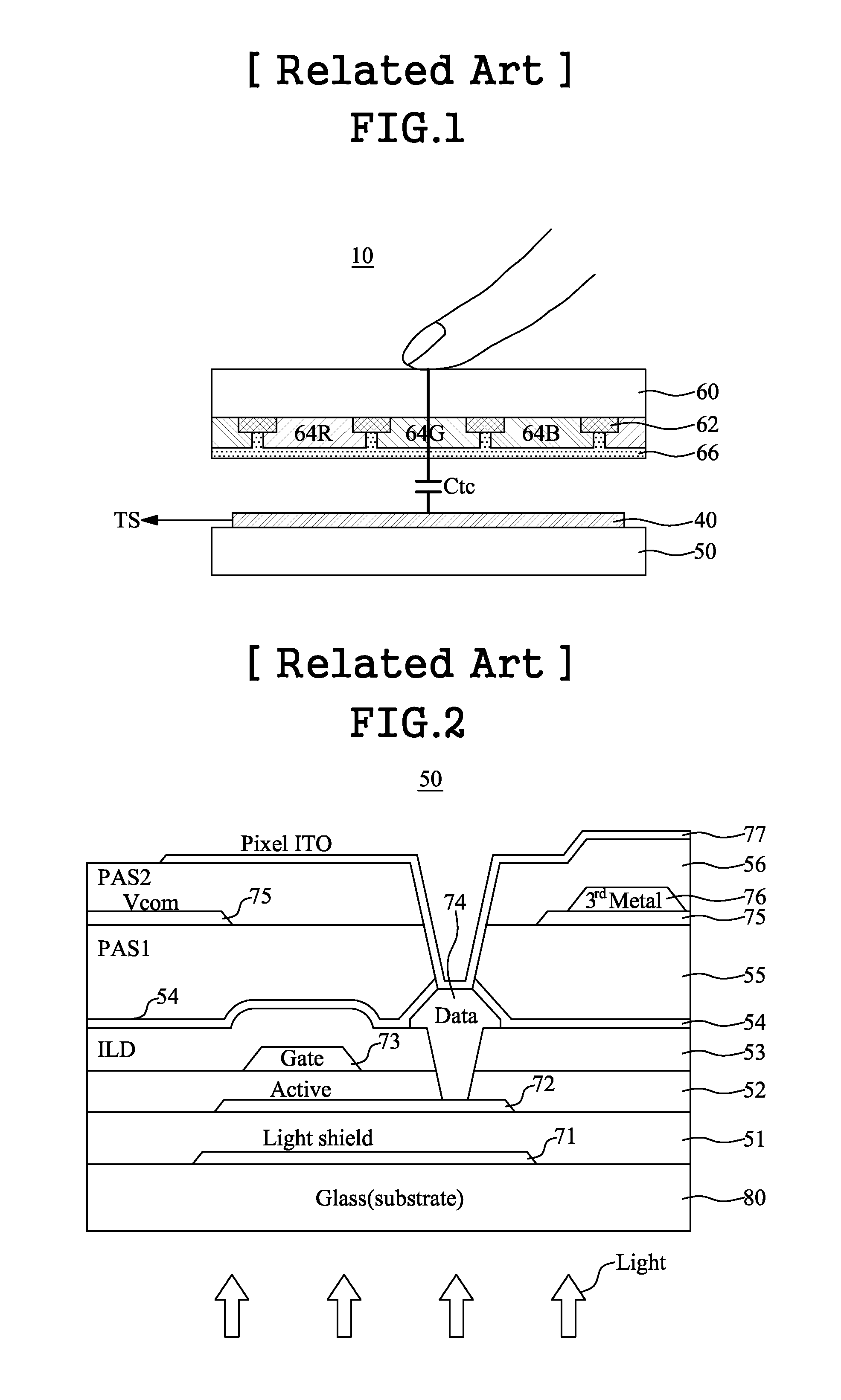
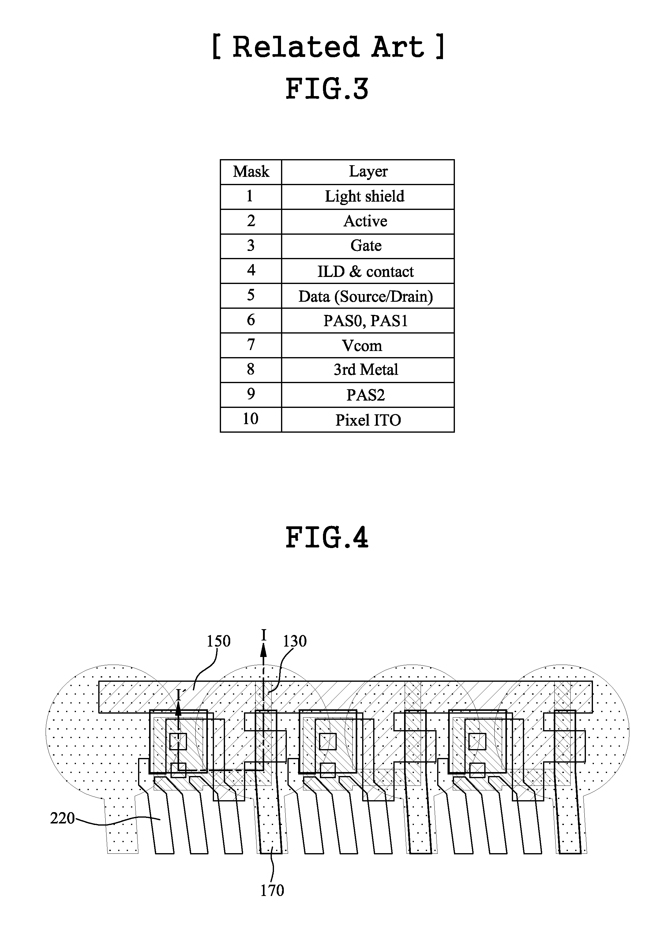
[0046]Depending on an alignment mode of liquid crystal layer, an LCD device may be classified into Twisted-Nematic (TN) mode, Vertical-Al...


PUM

PropertyMeasurementUnit
conductiveaaaaaaaaaa
Temperatureaaaaaaaaaa
sizeaaaaaaaaaa

Abstract

Disclosed is a liquid crystal display device with a built-in touch screen, which facilitates enhanced driving performance, and reduces manufacturing cost by a simplified manufacturing process, and a method for manufacturing the same. The device comprises a first substrate with a plurality of pixel regions defined by gate lines and data lines; an active layer in each pixel region of the first substrate; a gate pattern including a plurality of gate electrodes, a portion of the gate electrodes overlapping with a predetermined portion of the active layer with an insulating layer interposed in-between; a plurality of channel regions in the areas of the active layer overlapped with the plurality of gate electrodes; a plurality of lightly doped drain regions in the active layer and directly adjacent to the plurality of channel regions; and a data electrode electrically connected to the active layer.

Description

CROSS REFERENCE TO RELATED APPLICATIONS[0001]This application claims the benefit of the Korean Patent Application No. 10-2010-0092378 filed on Sep. 20, 2010, which is hereby incorporated by reference in its entirety as if fully set forth herein.BACKGROUND[0002]1. Field of the Disclosure[0003]The present disclosure relates to a flat panel display device, and more particularly, a liquid crystal display device with a built-in touch screen, which facilitates enhanced driving performance, and reduced manufacturing cost by simplifying the manufacturing process, and a method for manufacturing the same.[0004]2. Discussion of the Related Art[0005]According to development of various mobile electronic equipment, such as mobile terminals and notebook computers, there is increasing demand for a suitable flat panel display device. The flat panel display device may include an active-matrix liquid crystal display device (LCD), a plasma display panel (PDP), a field emission display device (FED), or ...

Claims


Application Information

Patent Timeline
Patent Type & Authority Applications(United States)
IPC IPC(8): G02F1/136H01L33/08
CPCH01L27/1214H01L29/42384G02F2001/136231H01L29/78696G02F1/13338H01L29/78645G02F1/136231
Inventor OH, KUM MILEE, HAN SEOKSHIN, HEE SUNPARK, WON KEUN
Owner LG DISPLAY CO LTD
Why Eureka
Try Eureka