Method for forming light emitting device

a technology of light-emitting devices and forming methods, which is applied in the direction of semiconductor devices, electrical devices, nanotechnology, etc., can solve the problems of long current path, high device resistance, and difficult to remove the generated hea

Active Publication Date: 2012-03-22
NAT TAIWAN UNIV
View PDF2 Cites 6 Cited by
  • Summary
  • Abstract
  • Description
  • Claims
  • Application Information

AI Technical Summary

Problems solved by technology

With the sapphire substrate, which is electrically and thermally insulating, such a light emitting device, however, has the disadvantage of long current path, such that the device resistance is high.
Also, the thermally insulating nature of sapphire substrate makes it difficult in removing the generated heat.
For example, laser irradiation may damage the material of the quantum wells in the light emitting diode.
Also, semiconductor chips are likely to be broken.

Method used


Image

  • Method for forming light emitting device
  • Method for forming light emitting device
  • Method for forming light emitting device

Examples


Embodiment Construction

[0020]It is understood that specific embodiments are provided as examples to teach the broader inventive concept, and one of ordinary skill in the art can easily apply the teaching of the present disclosure to other methods or apparatus. The following discussion is only used to illustrate the invention, not limit the invention.

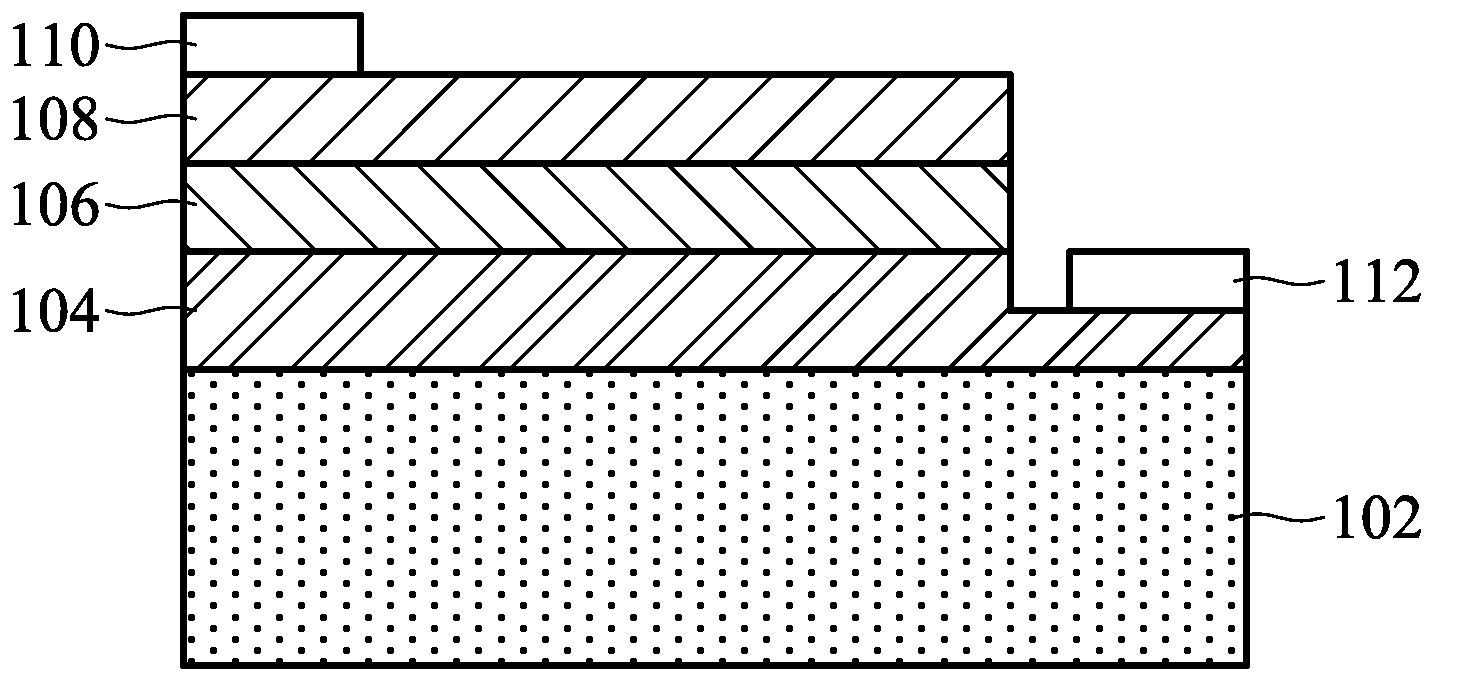
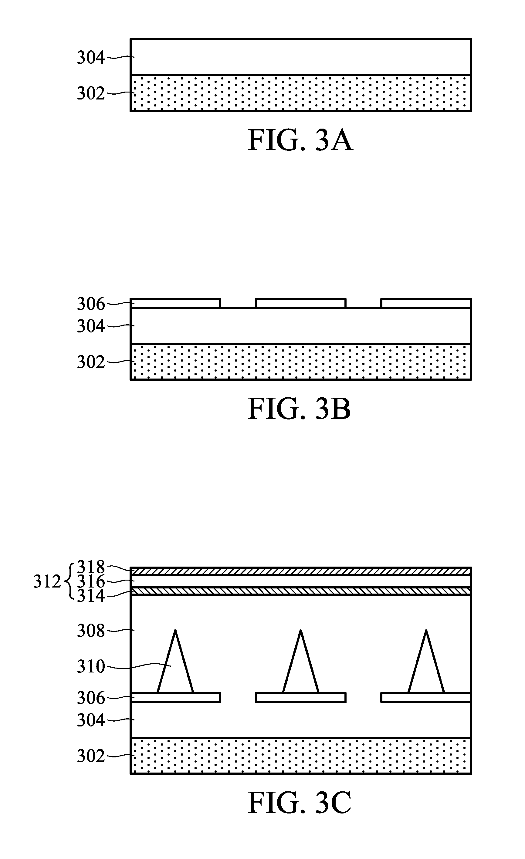
[0021]A method for forming a vertical light emitting diode of an embodiment of the invention is illustrated in accordance with FIGS. 3A˜3G. First, referring to FIG. 3A, a first substrate 302 such as sapphire substrate is provided. A semiconductor layer 304 is formed on the first substrate 302. In an embodiment of the invention, an undoped GaN layer with thickness of about 400 nm is deposited on the first substrate 302 by metal-organic chemical vapor deposition (MOCVD). Referring to FIG. 3B, a plurality of patterned masks 306 are formed on the undoped GaN layer 304. In an embodiment of the invention, the patterned mask layer 306 is a stripe-shaped silicon oxide...


PUM


Abstract

The invention provides a method for forming a light emitting device. A first substrate is provided. A plurality of patterned masks is formed on the first substrate, or on a semiconductor epitaxial layer grown on the first substrate, or the first substrate is etched to form a plurality of trenches, followed by performing an epitaxial lateral overgrowth process to grow an epitaxy layer over the first substrate. A light emitting structure is formed on the epitaxy layer. A first electrode layer is formed on the light emitting structure. The light emitting structure is wafer bonded to a second substrate. A photoelectrochemical etching process is performed to lift off the first substrate from the epitaxy layer.

Description

BACKGROUND OF THE INVENTION[0001]1. Field of the Invention[0002]This invention generally relates to methods for forming a light emitting device, and more particularly to a technique for lifting-off a sapphire substrate from a light-emitting diode.[0003]2. Description of the Related Art[0004]Semiconductor light-emitting devices have developed rapidly in many applications, for example, general lighting and liquid crystal display backlighting. As such, semiconductor light-emitting devices may replace currently used illumination devices, such as fluorescent lamps or light bulbs. Specifically, GaN based light-emitting diodes represent a main focus in such application developments. FIG. 1 shows the structure of a typical conventional light emitting device, wherein an n-GaN layer 104, quantum wells 106, and a p-GaN layer 108 are sequentially formed on a sapphire substrate 102, and a p-type electrode 110 connects to the p-GaN layer 108, and an n-type electrode 112 connects to the n-GaN laye...

Claims


Application Information

Patent Timeline
Patent Type & Authority Applications(United States)
IPC IPC(8): H01L33/48B82Y40/00
CPCB82Y40/00H01L21/0242H01L21/02458H01L21/0254H01L33/20H01L21/02647H01L21/02664H01L33/0079H01L21/02639H01L33/0093
Inventor YANG, CHIH-CHUNGLIN, CHENG-HUNGCHEN, CHIH-YENLIAO, CHE-HAOHSIEH, CHIEH
Owner NAT TAIWAN UNIV
Why Eureka
Try Eureka