Semiconductor device, method for manufacturing of semiconductor device, and switching circuit

a semiconductor device and semiconductor technology, applied in the direction of semiconductor devices, semiconductor/solid-state device details, electrical apparatus, etc., can solve the problems of leak current occurring when off and leak current cannot be ignored, and achieve the effect of lessening the concentration of electric fields

Active Publication Date: 2012-03-29
ADVANTEST CORP
View PDF21 Cites 10 Cited by
  • Summary
  • Abstract
  • Description
  • Claims
  • Application Information

AI Technical Summary

Benefits of technology

[0011]In the semiconductor device the ground side lead wiring may be adjacent to a ground side electrode, from among the plurality of ground side electrodes, that is closest to the ground side lead wiring, and the signal side lead wiring may be adjacent to a signal side electrode, from among the plurality of signal side electrodes, that is closest to the signal side lead wiring. The ground side electrode connecting section may lessen concentration of electric fields in the control electrodes. The ground side electrode connecting section may have a width greater than a width of the signal side electrode connecting section.

Problems solved by technology

A leak current also occurs between the gate electrode and the electrode pads.
However, HEMTs are used as DC switches as well as RF switches, and in this case, the leak current occurring when OFF cannot be ignored.

Method used


Image

  • Semiconductor device, method for manufacturing of semiconductor device, and switching circuit
  • Semiconductor device, method for manufacturing of semiconductor device, and switching circuit
  • Semiconductor device, method for manufacturing of semiconductor device, and switching circuit

Examples


embodiments

First Embodiment

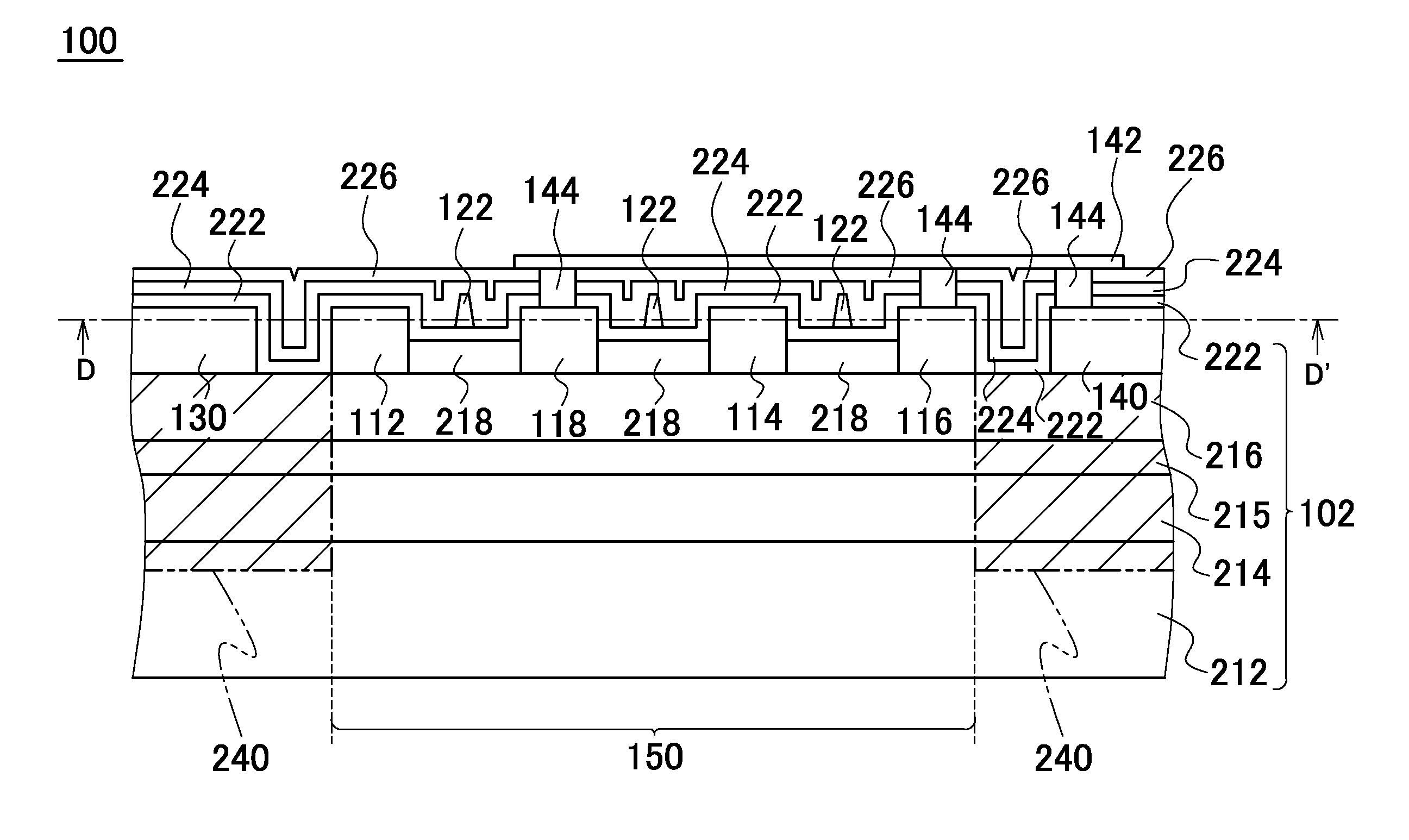
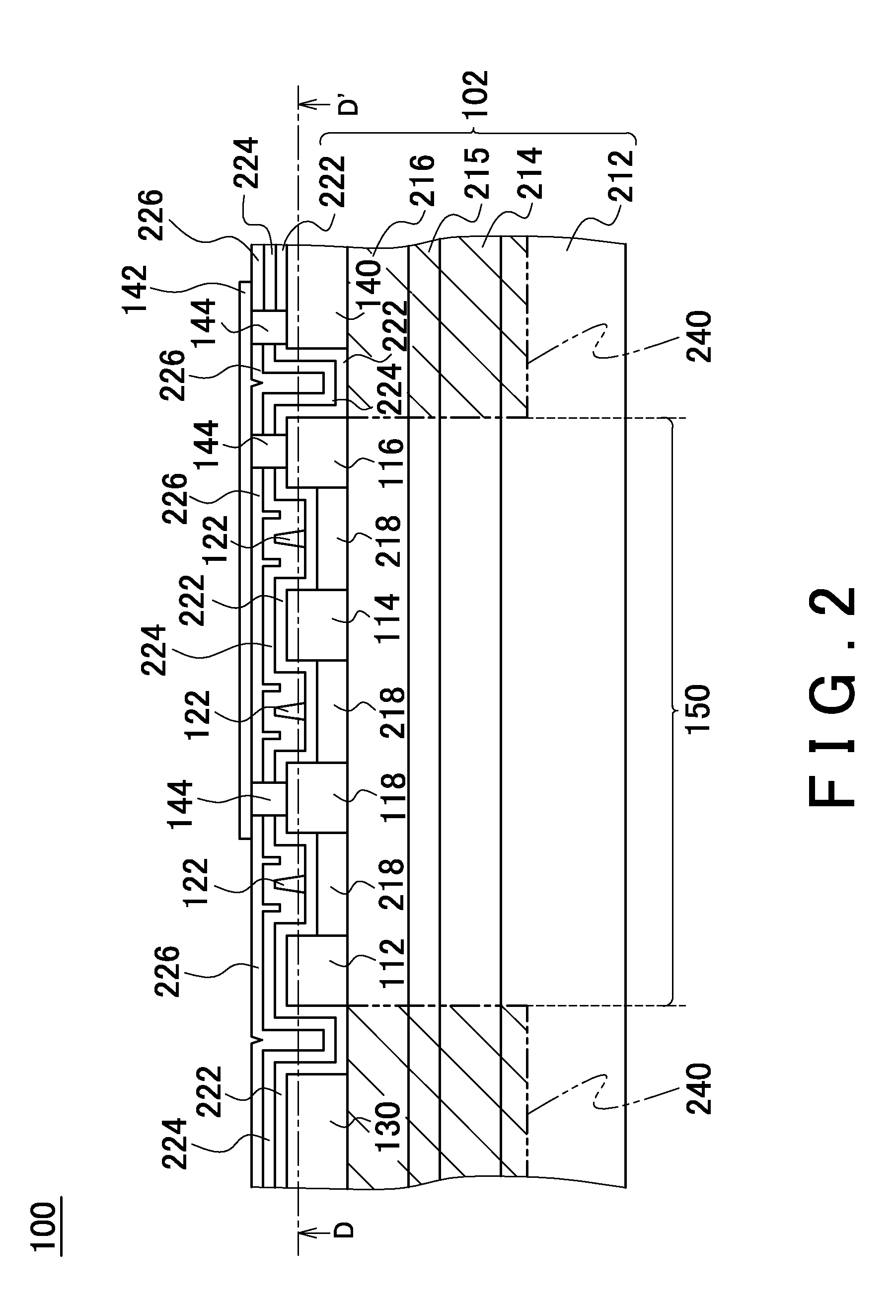
[0112]The HEMT 100 shown in FIGS. 1 to 3 was manufactured according to the steps described in relation to FIGS. 4 to 13. The substrate 102 was prepared in the following way. A commercial SiC substrate was prepared as the support substrate 212. Metal organic chemical vapor deposition (MOCVD) was used to form i-type GaN as the channel layer 214 on the SiC substrate. MOCVD was used to form i-type AlGaN as the spacer layer 215 on the channel layer 214.

[0113]MOCVD was used to form n-type AlGaN as the carrier supply layer 216 on the spacer layer 215. MOCVD was used to form n-type GaN as the cap layer 418 on the carrier supply layer 216, thereby creating the substrate 102. The cap layer 418 was patterned using etching to form the cap layer 218.

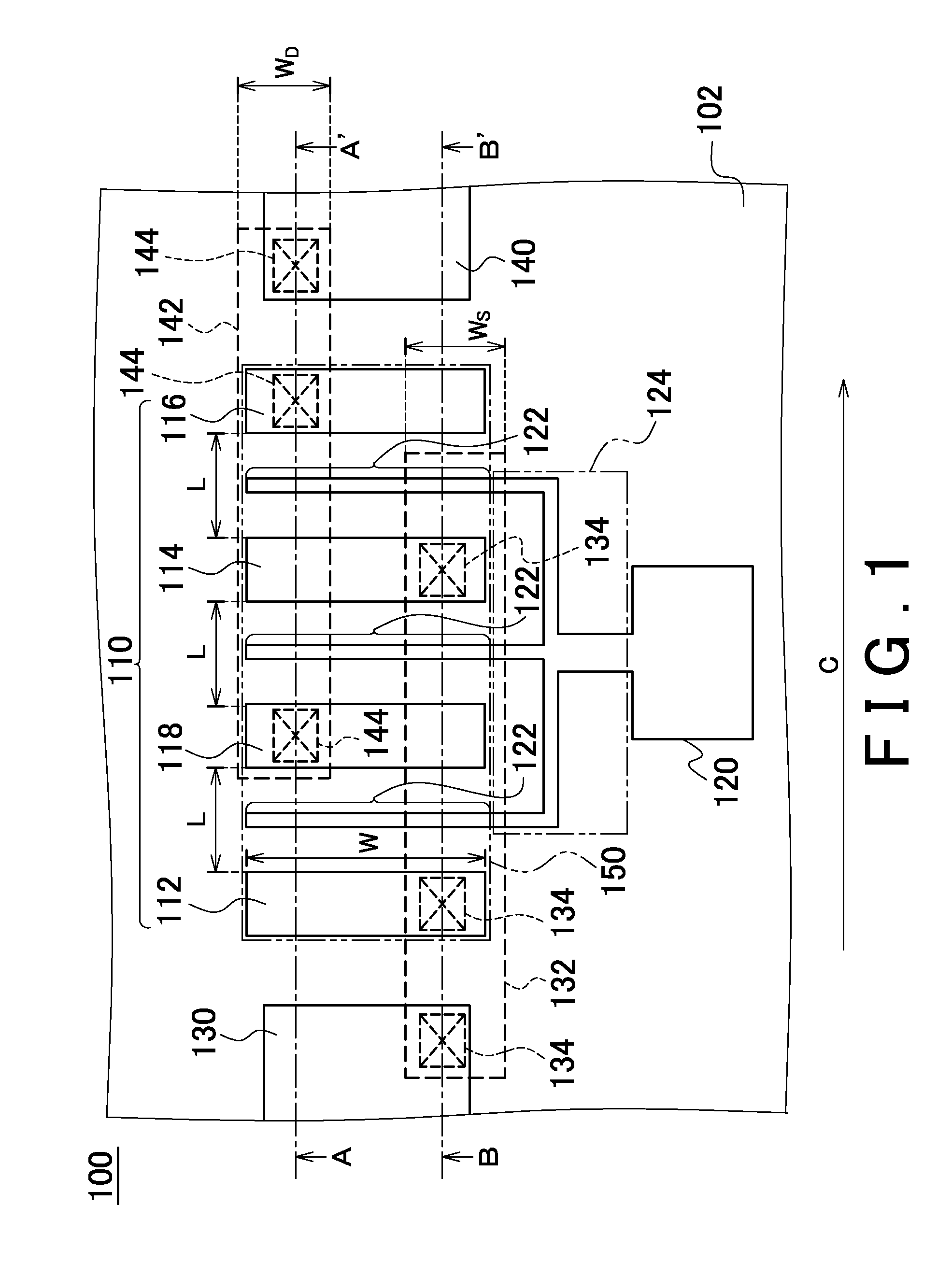
[0114]Next, a Ti thin film, an Al thin film, a Ni thin film, and a Au thin film were layered in the stated order on the prepared substrate 102 as each of the source electrode 112, the source electrode 114, the drain electrode 116, and...

second embodiment

[0119]The HEMT 1500 was manufactured in nearly the same manner as in the first embodiment. However, the second embodiment differs from the first embodiment in that, after forming the insulating layer 222, a portion of the insulating layer 222 was removed by etching. Furthermore, in the second embodiment, the step of forming the insulating layer 224 was omitted. In the same manner as the first embodiment, the second embodiment differs from the HEMT 100 shown in FIG. 15 by using a point-to-point construction for the source electrode connecting section 132 and the drain electrode connecting section 142.

third embodiment

[0120]The HEMT 1500 was manufactured in nearly the same manner as in the second embodiment. However, the third embodiment differs from the second embodiment in that CVD was used to form silicon nitride as the protective layer 226. In the third embodiment, when forming the silicon nitride, the temperature of the substrate 102 was set to 350° C.

[0121]FIG. 17 shows gate current characteristics of the HEMTs of the first and second embodiments. In FIG. 17, the vertical axis represents the gate current per 1 mm of gate width [A / mm], and the horizontal axis represents the gate voltage [V]. In FIG. 17, the reference numeral 1702 indicates experimental results of the first embodiment and the reference numeral 1704 indicates experimental results of the second embodiment.

[0122]As shown in FIG. 17, the HEMTs of the first and second embodiments both have gate currents held below 500 pA / mm in a gate voltage range from −30 V to 0 V. Furthermore, the gate currents are held below 250 pA / mm in a gate...


PUM


Abstract

It is an objective to provide a semiconductor device with low leak current. The semiconductor device includes a plurality of ground side electrodes and a plurality of signal side electrodes arranged on a semiconductor substrate in an alternating manner; a plurality of control electrodes arranged respectively between each pair of a ground side electrode and a signal side electrode; a ground side electrode connecting section that connects the ground side electrodes to each other; a signal side electrode connecting section that connects the signal side electrodes to each other; and ground side lead wiring and signal side lead wiring that extend respectively from a region near one end and a region near another end of an arranged electrode section, in which the ground side electrodes and the signal side electrodes are arranged in an arrangement direction, away from the arranged electrode group in the arrangement direction.

Description

BACKGROUND[0001]. Technical Field[0002]The present invention relates to a semiconductor device, a method of manufacturing the semiconductor device, and a switching circuit.[0003]2. Related Art[0004]A high electron mobility transistor (HEMT) using a compound semiconductor can operate at higher speeds than a silicon device. Because of this feature, an HEMT can be used as a device in a high-frequency switch (referred to hereinafter as an “RF switch”). Furthermore, the increasing frequencies of high-frequency switches have led to the development of HEMTs using comb-shaped gate electrodes.[0005]For example, Non-Patent Document 1 discloses an HEMT in which source electrodes and drain electrodes are arranged in an alternating manner, and a gate electrode is disposed between each pair of a source electrode and a drain electrode. Furthermore, the HEMT of Non-Patent Document 1 includes a source side electrode pad and a drain side electrode pad that extend in the direction of the channel lengt...

Claims


Application Information

Patent Timeline
Patent Type & Authority Applications(United States)
IPC IPC(8): H01L23/48H01L21/28
CPCH01L29/0696H01L29/2003H01L29/42376H01L29/66462H01L2924/0002H01L29/7787H01L2924/00
Inventor NAKANISHI, MAKOTOYAMANOUCHI, TOMOOOKAYASU, JUNICHISATO, TAKUTERASAWA, DAIJUTAKIKAWA, MASAHIKO
Owner ADVANTEST CORP
Why Eureka
Try Eureka