Electromechanical transducer and method of manufacturing the same

a technology of electromechanical transducers and manufacturing methods, applied in mechanical vibration separation, semiconductor devices, electrical apparatus, etc., can solve the problems of reducing the stiffness of the transducer array, oxidizing monocrystalline silicon diaphragms, and breaking of the transducer array, so as to prevent the lowering of the stiffness of the transducer and reduce the thickness fluctuations. , the effect of small residual stress

Inactive Publication Date: 2012-04-19
CANON KK
View PDF4 Cites 43 Cited by
  • Summary
  • Abstract
  • Description
  • Claims
  • Application Information

AI Technical Summary

Benefits of technology

[0011]According to the present invention, the electromechanical transducer has a configuration that the through wiring for electrical connection to the semiconductor film including the diaphragm is taken out to the opposite side of the semiconductor substrate, and the substrate is not divided, and thus, the lowering of the stiffness of the transducer is prevented.
[0012]The electromechanical transducer having such a configuration may be manufactured by the manufacturing method according to the present invention described above, in which a semiconductor material such as monocrystalline silicon having small thickness fluctuations and having small residual stress is used as a main material of a diaphragm, and the diaphragm is formed on one surface side of the semiconductor substrate. Thus, spring constant fluctuations and deformation fluctuations in the diaphragm can be reduced, and an electromechanical transducer having high consistency among elements and having reduced transmission and reception performance fluctuations may be provided.
[0013]Further, in the method of manufacturing an electromechanical transducer according to the first aspect of the present invention, a through wiring for electrical connection to a semiconductor film including the diaphragm is formed. Thus, an electromechanical transducer with high stiffness can be easily manufactured. Further, since a protective film is formed on the semiconductor film including the diaphragm before an insulating layer is formed in a through hole, the diaphragm is not exposed outward when the through wiring is formed, and an insulating layer material may be prevented from depositing directly on the diaphragm. Thus, since the spring constant fluctuations and the deformation fluctuations in the diaphragm may be reduced, and, an electromechanical transducer having high performance consistency can be provided. Here, when polysilicon or the like is used as a conductor material for the wiring, in order to prevent the conductor material from depositing on the diaphragm, the diaphragm may preferably be protected by a protective film also when the conductor is formed on the insulating layer in the through hole.
[0014]Further, according to the method of manufacturing an electromechanical transducer according to the second aspect of the present invention, a through wiring for electrical connection to the rear surface of a semiconductor film including the diaphragm is formed. Thus, an electromechanical transducer having high stiffness can be easily manufactured. Further, since the diaphragm is not exposed when the through wiring is formed, an insulating layer material and a conductor material used in forming the through wiring may be prevented from depositing directly on the diaphragm. Thus, the spring constant fluctuations and the deformation fluctuations in the diaphragm may be reduced. Further, since no through hole is formed in the front surface of the electromechanical transducer, the liquid may be prevented from entering the rear surface of the electromechanical transducer when the electromechanical transducer is used in a liquid.

Problems solved by technology

However, since the silicon substrate is divided, the stiffness of the transducer array is lowered and the transducer array may be broken by thermal stress in mounting or the like.
Further, when thermally oxidizing a through hole, the monocrystalline silicon diaphragm may also be oxidized.
This may cause thickness fluctuations in the diaphragm or generate stress thereon.
Further, when polysilicon is used as a conductor for the wiring, the polysilicon may also deposit on the monocrystalline silicon diaphragm, which may result in thickness fluctuations in the diaphragm and stress on the diaphragm.
It may lead to lower consistency among elements in which transducer cells are included, and performance fluctuations among the elements in the capacitive transducer array may be increased.

Method used


Image

  • Electromechanical transducer and method of manufacturing the same
  • Electromechanical transducer and method of manufacturing the same
  • Electromechanical transducer and method of manufacturing the same

Examples


example 1

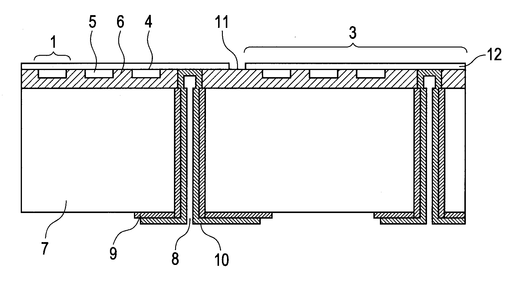
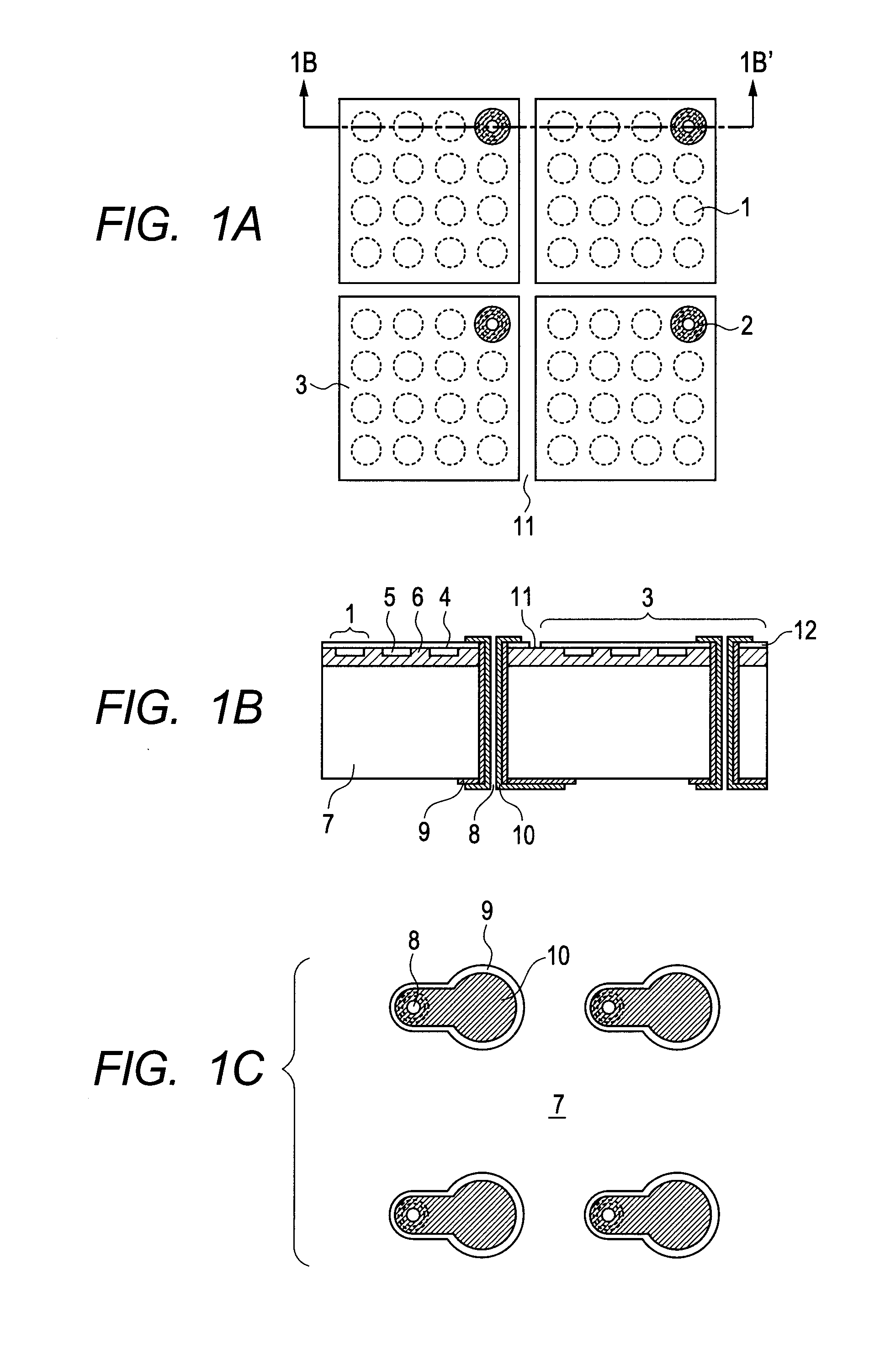
[0060]A configuration of a capacitive transducer array of Example 1 is described with reference to FIGS. 1A to 1C used in describing the above-mentioned first embodiment. In this example, too, the capacitive transducer array includes multiple elements 3 each including multiple cellular structures 1 and through wiring 2. In FIG. 1A, only four of the elements 3 are illustrated, but arbitrary number of the elements 3 may be arranged.

[0061]The cellular structure 1 includes a monocrystalline silicon diaphragm 4 having a thickness of 1 μm, a gap 5, a diaphragm supporting portion 6 for supporting the monocrystalline silicon diaphragm 4 having a resistivity of 0.01 Ω·cm, and a silicon substrate 7. The silicon substrate 7 has a thickness of 300 μm and a resistivity of 0.01 Ω·cm. The cellular structure 1 illustrated in FIGS. 1A to 1C is in the shape of a circle, but may be in the shape of a square, a hexagon, or the like. A main material of the monocrystalline silicon diaphragm 4 is monocryst...

example 2

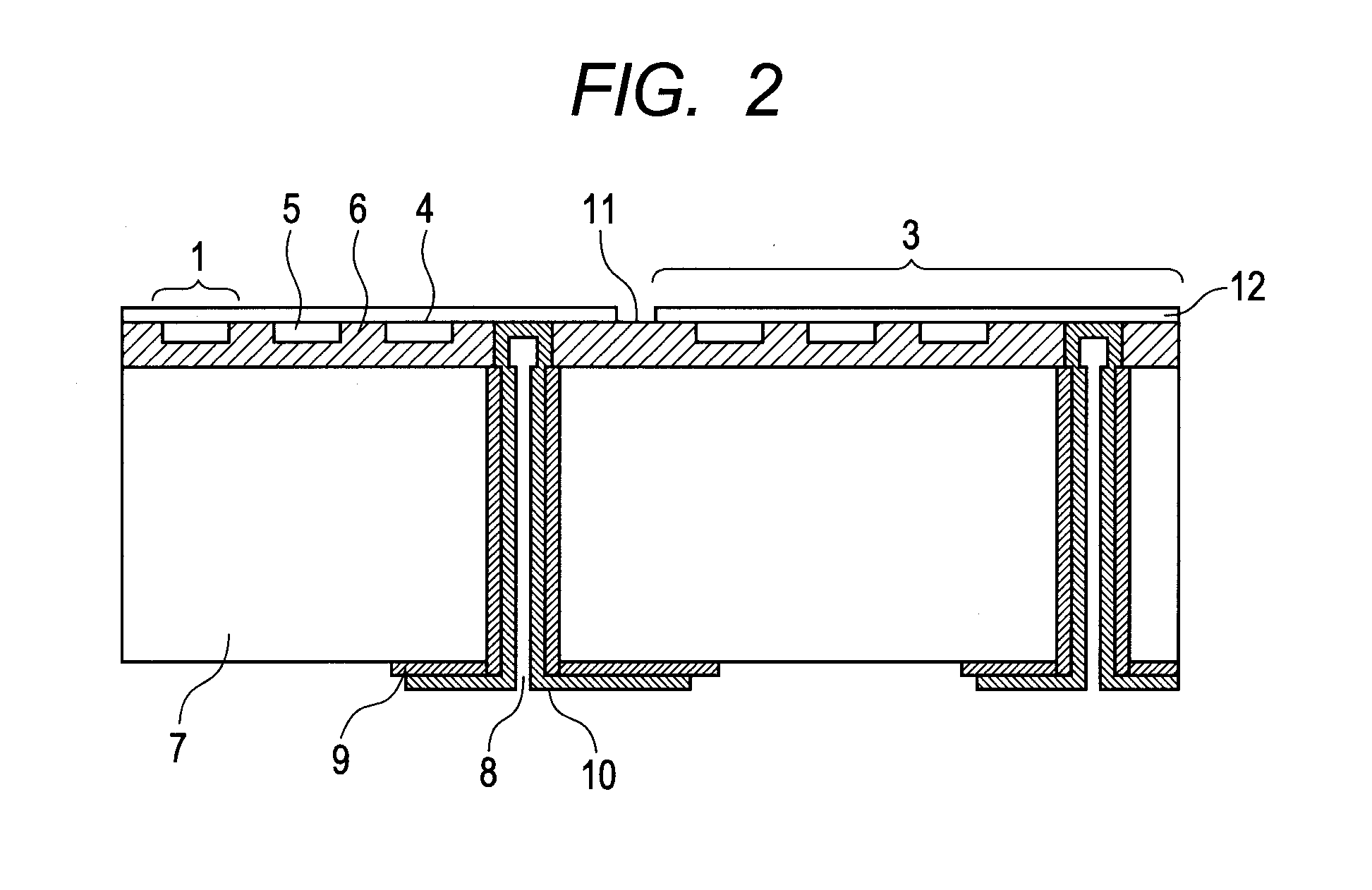
[0067]A configuration of a capacitive transducer array of Example 2 is described with reference to FIG. 2. FIG. 2 is a sectional view of the capacitive ultrasound transducer array of this example. The configuration of Example 2 is substantially similar to that of Example 1.

[0068]A cellular structure 1 includes a monocrystalline silicon diaphragm 4 having a thickness of 1 μm, a gap 5, a diaphragm supporting portion 6 for supporting the monocrystalline silicon diaphragm 4, and a silicon substrate 7. The silicon substrate 7 has a thickness of 300 μm and a resistivity of 0.01 Ω·cm. In this configuration, the cellular structure 1 is in the shape of a circle with the diameter of 40 μm. The diaphragm supporting portion 6 is formed of silicon oxide and has a height of 400 nm. The amount of the gap 5 is 200 nm. The through wiring 2 includes a through hole 8, a conductor 10, and an insulating layer 9 for insulating the side wall of the through hole 8 and a part of the silicon substrate 7 from...

example 3

[0070]A method of manufacturing a capacitive transducer array of Example 3 is described with reference to FIGS. 3A to 3F used in describing the above-mentioned first embodiment. As illustrated in FIG. 3A, an insulating layer 31 which is silicon oxide is formed by thermal oxidation on a first silicon substrate 30 having a thickness of 300 μm, and a gap 32 is formed by photolithography or etching. The resistivity of the first silicon substrate 30 is on the order of 0.01 Ω·cm.

[0071]Then, as illustrated in FIG. 3B, a second silicon substrate 33 is bonded and thinned. Here, the second silicon substrate 33 is an SOI substrate. In the SOI substrate, an active layer 34 has a thickness of 1 μm, a BOX layer 35 has a thickness of 0.4 μm, and a handle layer 36 has a thickness of 525 μm. The active layer 34 in the SOI substrate has a resistivity of 0.1 Ω·cm. The active layer 34 having thickness fluctuations of ±5% or less is used, and the active layer side is directly bonded. The active layer in...


PUM

PropertyMeasurementUnit
resistivityaaaaaaaaaa
thicknessaaaaaaaaaa
thicknessaaaaaaaaaa

Abstract

An electromechanical transducer includes multiple elements each including at least one cellular structure, the cellular structure including: a semiconductor substrate, a semiconductor diaphragm, and a supporting portion for supporting the diaphragm so that a gap is formed between one surface of the substrate and the diaphragm. The elements are separated from one another at separating locations of a semiconductor film including the diaphragm. Each of the elements includes in a through hole passing through a first insulating layer including the supporting portion and the semiconductor substrate: a conductor which is connected to the semiconductor film including the diaphragm; and a second insulating layer for insulating the conductor from the semiconductor substrate.

Description

BACKGROUND OF THE INVENTION[0001]1. Field of the Invention[0002]The present invention relates to an electromechanical transducer such as a capacitive transducer array, and to a method of manufacturing the electromechanical transducer.[0003]2. Description of the Related Art[0004]Conventionally, micromechanical members to be manufactured using micromachining technology may be processed on the order of micrometers, and various functional microelements are materialized using such micromechanical members. A capacitive transducer using such technology (CMUT: capacitive micromachined ultrasonic transducer) is being studied as an alternative to a piezoelectric element. With such a CMUT, ultrasound may be transmitted and received using vibrations of a diaphragm, and in particular, excellent wide-band characteristics in a liquid can be obtained with ease.[0005]With regard to the above-mentioned technology, there is a capacitive transducer array in which a silicon nitride film is formed on a s...

Claims


Application Information

Patent Timeline
Patent Type & Authority Applications(United States)
IPC IPC(8): H01L29/84H01L21/02
CPCB81C1/00158B06B1/0292
Inventor TORASHIMA, KAZUTOSHIAKIYAMA, TAKAHIRO
Owner CANON KK
Why Eureka
Try Eureka