

Fabricating kesterite solar cells and parts thereof
- Summary
- Abstract
- Description
- Claims
- Application Information
AI Technical Summary
Benefits of technology
Method used
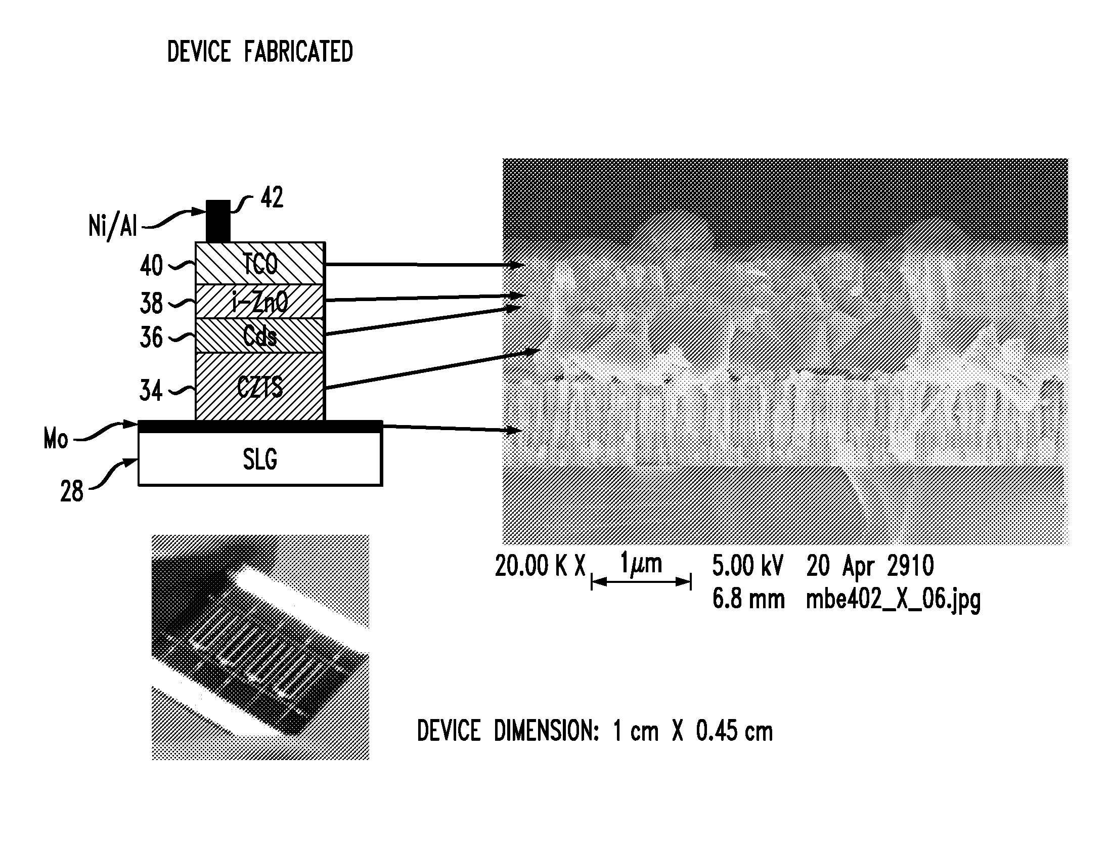
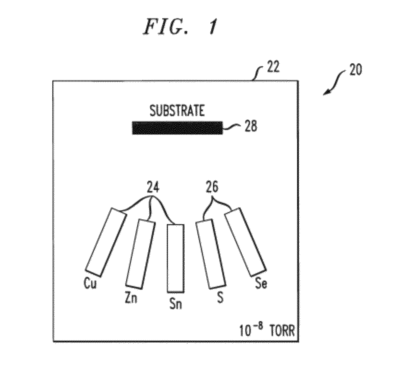
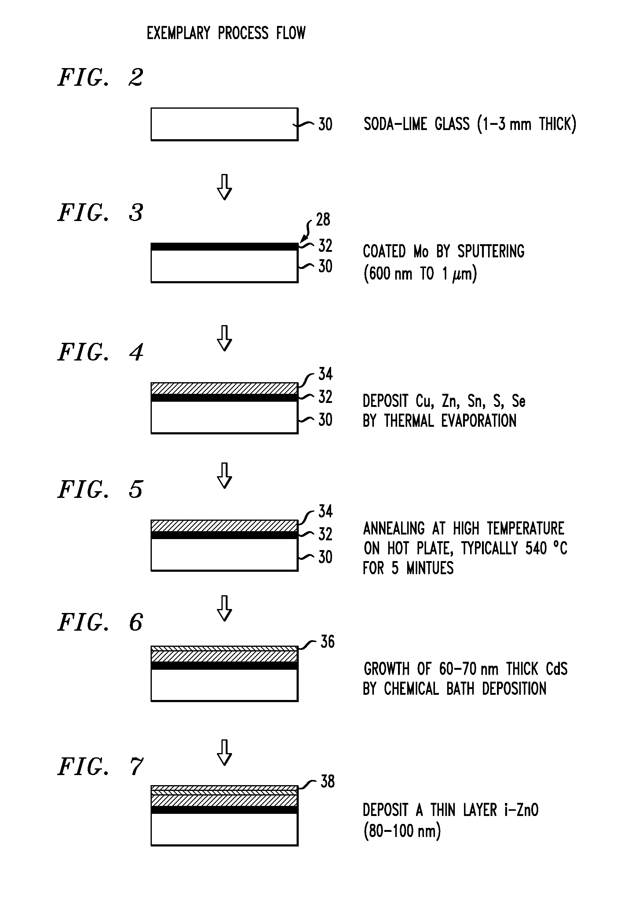
Image

Examples
Embodiment Construction
[0020]Kesterite, also known as Cu2ZnSnSxSe4-x, or CZTSSe, holds the promise of low-cost, renewable solar cells since all the elements used are inexpensive and earth-abundant. Unlike CIGS absorbers, which require the relatively expensive elements indium and gallium, zinc and tin are readily available at reasonable prices, kesterite films have been deposited by various techniques, including thermal evaporation, solution processes, electroplating, sputtering, and the like. Solution processes can require hydrazine which is both explosive and toxic. Sputtering techniques and electroplating typically involve the deposit of Cu / Zn / Sn alloy followed by annealing with H2S or S for more than two hours.
[0021]Most fabrication flows require high temperature annealing (>500° C.) to grow large grains for the kesterite absorber layer. Commonly used methods for high temperature annealing include annealing in a furnace with flowing H2S gas, and annealing inside a sealed tube with sufficient S vapor pr...
PUM
 Abstract
Description
Claims
Application Information