

Replacement gate mosfet with raised source and drain
- Summary
- Abstract
- Description
- Claims
- Application Information
AI Technical Summary
Benefits of technology
Problems solved by technology
Method used
Image

Examples
first embodiment
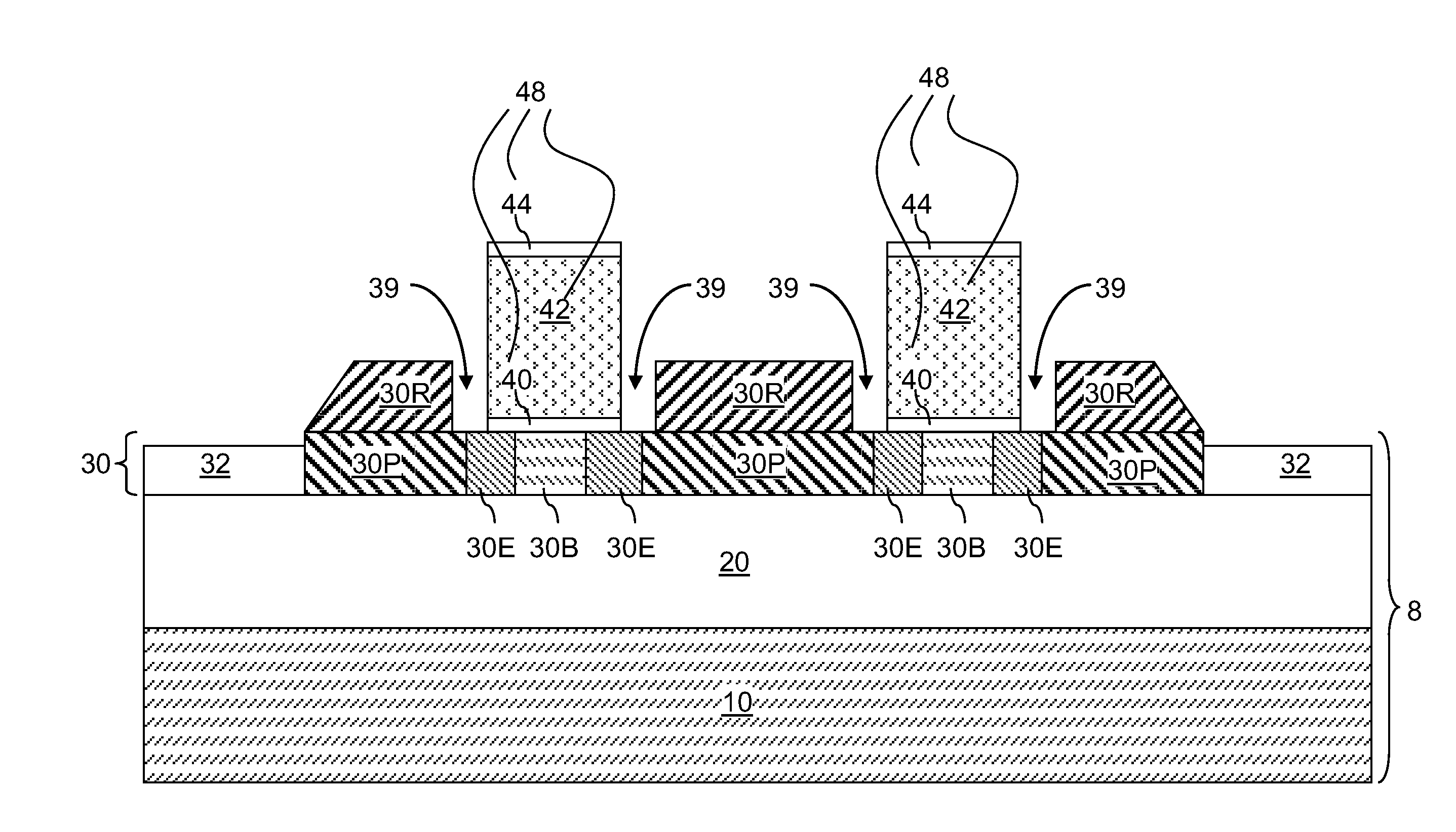
[0016]Referring to FIG. 1, a first exemplary semiconductor structure according to the present disclosure includes a semiconductor substrate 8. The semiconductor substrate 8 can be a bulk semiconductor substrate including an active region 30L and isolation structures 32, or can be a semiconductor-on-insulator (SOI) substrate including a stack, from bottom to top, of a handle substrate 10, a buried insulator layer 20, and a top semiconductor layer 30 that includes an active region 30L and isolation structures 32. The active region 30L can be a single crystalline semiconductor material portion in which semiconductor atoms are epitaxially aligned to one another in the entirety thereof. The isolation structures 32 include a dielectric material such as silicon oxide and / or silicon nitride. For example, the isolation structures 32 can be shallow trench isolation structures known in the art. In one embodiment, the SOI substrate can be an ultrathin SOI substrate in which the thickness of the...
second embodiment
[0054]Referring to FIG. 8, second exemplary semiconductor structure according to the present disclosure is derived from the first exemplary semiconductor structure of FIG. 6 by forming a dielectric gate spacer 52 on sidewalls of each gate cavity 59.
[0055]As discussed above, vertical surfaces of the gate-level dielectric layer 50 are exposed on the sidewalls of each gate cavity 59 upon removal of the at least one the disposable material stack 48. The at least one dielectric gate spacer 52 can be formed by depositing a conformal dielectric material layer and anisotropically etching horizontal portions of the conformal dielectric material layer. The remaining vertical portions of the conformal dielectric material layer become the at least one dielectric gate spacer 52. The at least one dielectric gate spacer 52 includes a dielectric material such as silicon oxide, silicon nitride, silicon oxynitride, organosilicate glass (OSG), or a combination thereof.
[0056]Referring to FIG. 9, the pr...
PUM
 Abstract
Description
Claims
Application Information