Copper foil with resistance layer, method of production of the same and laminated board

a technology of copper foil and resistance layer, which is applied in the direction of superimposed coating process, core/yokes, transportation and packaging, etc., can solve the problems of high ratio of employment of copper foil, difficult to obtain a uniform distribution of roughening particles on the surface of copper foil by fine roughening treatment, etc., to achieve small variation of resistance value, and suitable elasticity and plasticity

Inactive Publication Date: 2012-05-10
FURUKAWA ELECTRIC CO LTD
View PDF13 Cites 23 Cited by
  • Summary
  • Abstract
  • Description
  • Claims
  • Application Information

AI Technical Summary

Benefits of technology

[0023]According to the copper foil with a resistance layer of the present invention, it is possible to provide a copper foil with a resistance layer having a small variation of resistance values as a resistance element, being capable of sufficiently maintaining the JPCA standard (JPCA-EB01) regarding the adhesion with the resin substrate to be laminated, and having suitable elasticity and plasticity and folding resistance so as to be capable of match with bending in a range of R=0.8 to 1.25 (mm).
[0024]Further, according to the method of production of the copper foil with a resistance layer of the present invention, it is possible to produce a copper foil with resistance layer having a small variation of resistance values even in a case where it is processed to a resistance element, being capable of sufficiently maintaining the JPCA standard (JPCA-EB01) regarding the adhesion with the resin substrate to be laminated, and having suitable elasticity and plasticity and folding resistance so as to be capable of match with bending in a range of R=0.8 to 1.25 (mm).
[0025]According to the laminated board of the present invention, it is possible to provide a laminated board formed by laminating a resin substrate and a copper foil with a resistance layer, being capable of sufficiently maintaining the JPCA standard (JPCA-EB01) regarding the adhesion with the resin substrate, and having a small variation of resistance value.

Problems solved by technology

However, resistors, capacitors, inductances, etc. corresponding to passive devices are restricted in processing conditions as opposed to active elements.
In the metal foil of the metal foil with a resistance layer, the ratio of employment of copper foil is high due to both of handling processability and cost performance when the method of formation of the resistance layer (thin film) is either electroplating type or sputtering type.
However, it is difficult to obtain a uniform distribution of roughening particles on the surface of the copper foil by the fine roughening treatment.
This causes the problem of a larger variation in individual resistance values obtained in the in-plane resistance value measurement method prescribed in JIS-K-7194.
Consequently, even if a resistance element pattern is formed along the circuit design, there is a possibility that the theoretical resistance value will not be obtained.

Method used


Image

  • Copper foil with resistance layer, method of production of the same and laminated board
  • Copper foil with resistance layer, method of production of the same and laminated board
  • Copper foil with resistance layer, method of production of the same and laminated board

Examples


example 1

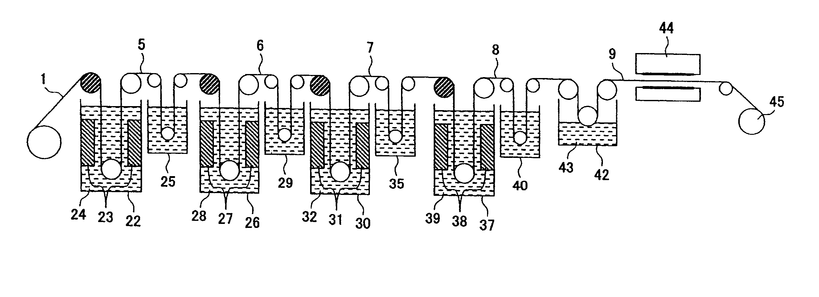
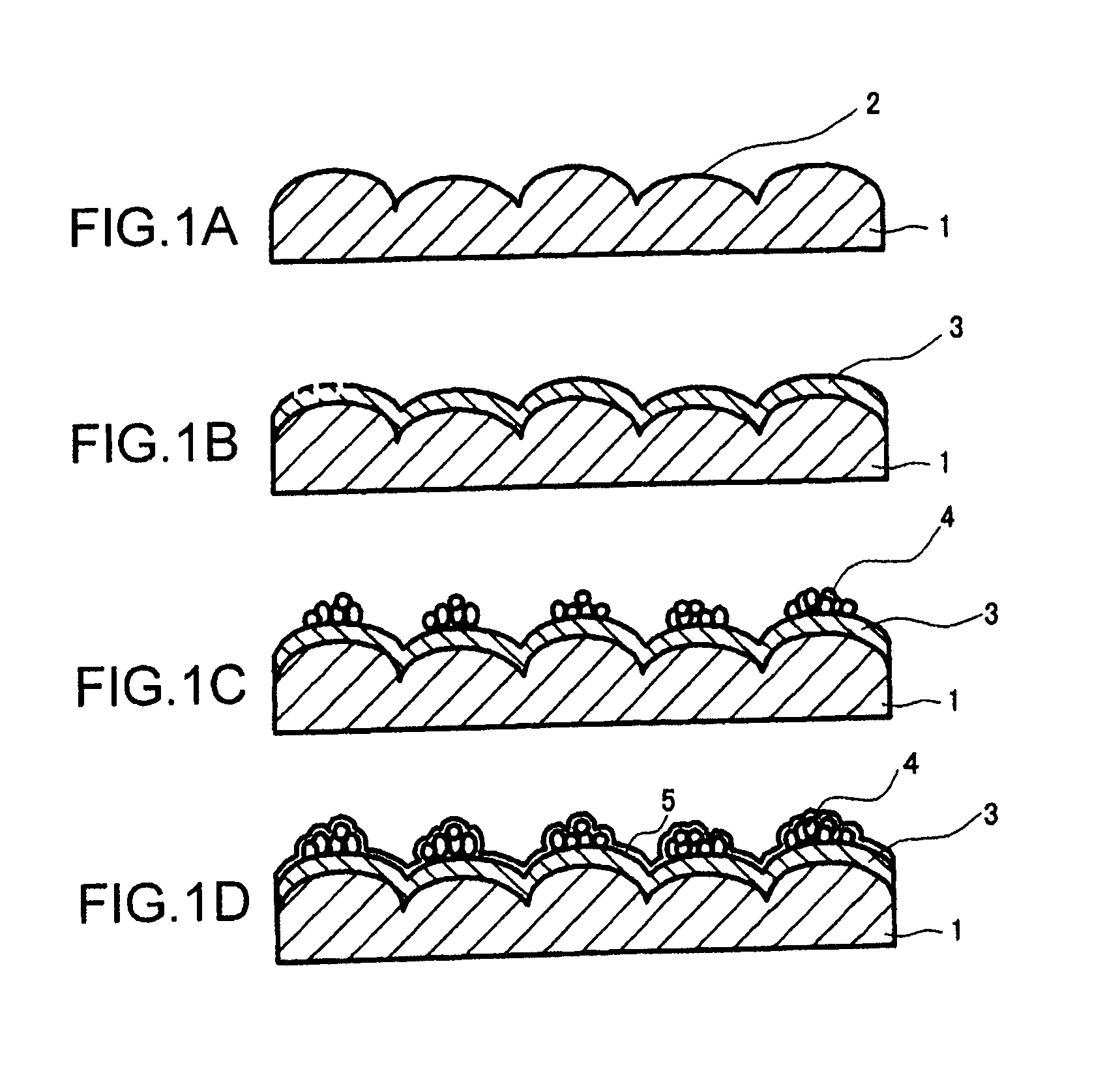
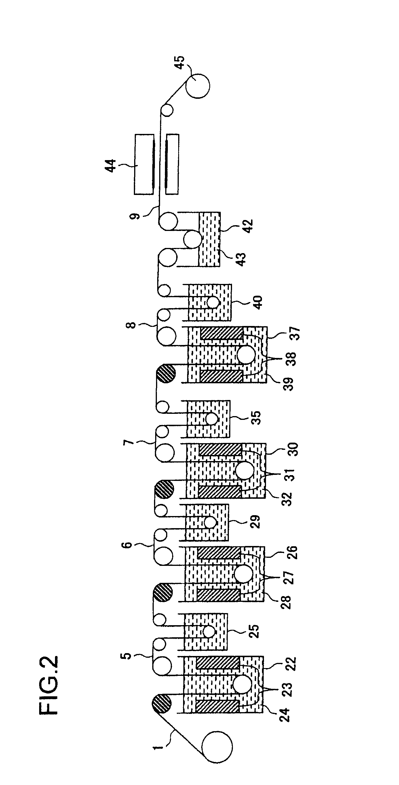
[0059]Use was made of copper foil (MP foil made by Furukawa Electric Co., Ltd.) which was produced under electrodepositing foil production conditions, had a thickness of 18 μm, had a shape roughness on the matte surface side (electrolytic solution surface side) of 4.8 μm in terms of the Rz value prescribed in JIS-B-0601, and had an elongation after heating at 180° C. for 60 minutes under atmospheric heating conditions of 14.2% so as to form a resistance layer thin film for forming a resistance element body on the matte surface side, perform nickel roughening treatment, and perform capsule plating treatment under the following conditions.

[0060][Resistance Layer-Forming Bath Composition and Treatment Conditions]

[0061]As nickel, using nickel sulfamate . . . 65 g / l

[0062]As PO3 of phosphorous acid . . . 40 g / l

[0063]As PO4 of hypophosphorous acid . . . 50 g / l

[0064]Boric acid (HBO3) . . . 30 g / l

[0065]pH: 1.6

[0066]Bath temperature: 55° C.

[0067]Electroplating current density . . . 5.0 A / dm2 ...

example 2

[0086]Except for the use of a copper foil (MP foil produced by Furukawa Electric Co., Ltd.) which was produced under electrodepositing foil production conditions, had a thickness of 18 μm, had a shape roughness on the matte surface side of 4.5 μm in terms of Rz value prescribed in JIS-B-0601, and had an elongation after heating at 180° C. for 60 minutes under atmospheric heating conditions of 14.2%, treatments were carried out under the conditions described in Example 1 for subjecting to the evaluation and measurement.

[0087]The results of measurement and evaluation are described in Table 1.

example 3

[0088]Except for the use of a copper foil (MP foil produced by Furukawa Electric Co., Ltd.) which was produced under electrodepositing foil production conditions, had a thickness of 18 μm, had a shape roughness on the matte surface side of 4.5 μm in terms of Rz value prescribed in JIS-B-0601, and had an elongation after heating at 180° C. for 60 minutes under atmospheric heating conditions of 12.0%, treatments were carried out under the conditions described in Example 1 for subjecting to the evaluation and measurement.

[0089]The results of measurement and evaluation are described in Table 1.


PUM

PropertyMeasurementUnit
elongationaaaaaaaaaa
temperatureaaaaaaaaaa
roughnessaaaaaaaaaa

Abstract

A copper foil with a resistance layer is provided, wherein the variation value is small when it is made into a resistance element, the adhesion with the resin substrate to be laminated with is able to be sufficiently maintained, which has an excellent characteristics as a resistance element for a rigid and a flexible substrate. A copper foil with a resistance layer of the present invention comprises a copper foil on one surface of which a metal layer or alloy layer is formed from which a resistance element is to be formed, the surface of the metal layer or alloy layer being subjected to a roughening treatment with nickel particles. A method of production of a copper foil with a resistance layer of the present invention comprises: forming a resistance layer of phosphorus-containing nickel on a matte surface of an electrodeposited copper foil having crystals comprised of columnar crystal grains wherein a foundation of the matte surface is within a range of 2.5 to 6.5 μm in terms of Rz value prescribed in JIS-B-0601; and performing roughening treatment to a surface of the resistance layer with nickel particles wherein a roughness is within a range of 4.5 to 8.5 μm in terms of Rz value prescribed in JIS-B-0601. The alloy layer is for example formed from phosphorus-containing nickel.

Description

TECHNICAL FIELD[0001]The present invention relates to a copper foil with a resistance layer which reduces variation of the resistance value and has excellent characteristics as a resistance element for a rigid substrate and a flexible substrate, a method of production of the same, and a laminated board using the same.BACKGROUND ART[0002]Mobile electronic terminals as typified by mobile phones, even compared with electronic devices in general, have in recent years been increasingly made smaller in size and thinner in thickness and additionally been made remarkably more advanced in functions enabling them to not only handle phone calls, but also send and receive images and moving pictures of course and also provide GPS (global positioning system) functions, 1 SEG television reception, and other functions. Along with this increase in functions, the components of the mobile terminals are becoming strikingly more modularized. How to reduce the size of modules having one or more functions...

Claims


Application Information

Patent Timeline
Patent Type & Authority Applications(United States)
IPC IPC(8): H05K1/09C23C28/02B32B15/04H05K1/02B32B15/01
CPCC23C30/00C25D1/04C25D3/562C25D5/34C25D5/48C25D7/0628Y10T428/12076H05K1/167H05K3/384H05K3/389H05K2201/0355H05K2203/0307Y10T428/12049C25D11/38C25D5/605C25D5/617
Inventor OGURO, RYOICHIKASE, KOUJIHOSHINO, KAZUHIRO
Owner FURUKAWA ELECTRIC CO LTD
Why Eureka
Try Eureka