Method for forming a semiconductor device using selective epitaxy of group iii-nitride

Inactive Publication Date: 2012-05-17
APPLIED MATERIALS INC
View PDF0 Cites 127 Cited by
  • Summary
  • Abstract
  • Description
  • Claims
  • Application Information

AI Technical Summary

Problems solved by technology

The c-plane of a Group III-Nitride is polar and has a piezoelectric field; both properties can affect device performance due to energy band distortion, separation of electrons and holes, and reduction of the radiative recombination efficiency.
However, films grown in the direction of these planes typically have a higher threading disloc

Method used


Image

  • Method for forming a semiconductor device using selective epitaxy of group iii-nitride
  • Method for forming a semiconductor device using selective epitaxy of group iii-nitride
  • Method for forming a semiconductor device using selective epitaxy of group iii-nitride

Examples


Embodiment Construction

[0035]Embodiments of the present invention include a method of forming one or more Group III-Nitride films on a patterned substrate. Other embodiments include employing the Group III-Nitride film as a basis for a semiconductor device, such as a light emitting diode (LED), laser diode, high electron mobility transistors (HEMTs), hetero junction bipolar transistors (HBTs) and quantum well devices. The present invention has been described with respect to specific details in order to provide a thorough understanding of the invention. One of ordinary skill in the art will appreciate that the invention can be practiced without these specific details. In other instances, well known semiconductor processes and equipment have not been described in specific detail in order to not unnecessarily obscure the present invention.

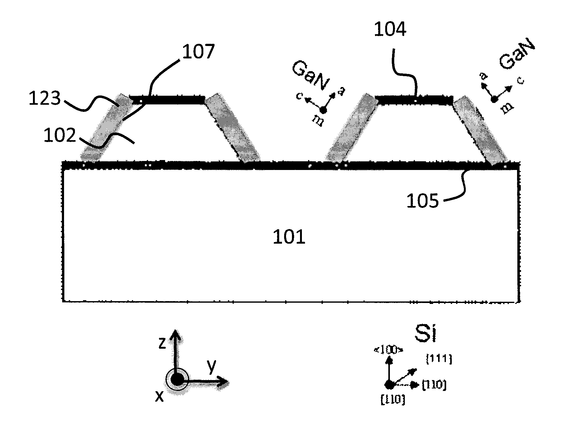
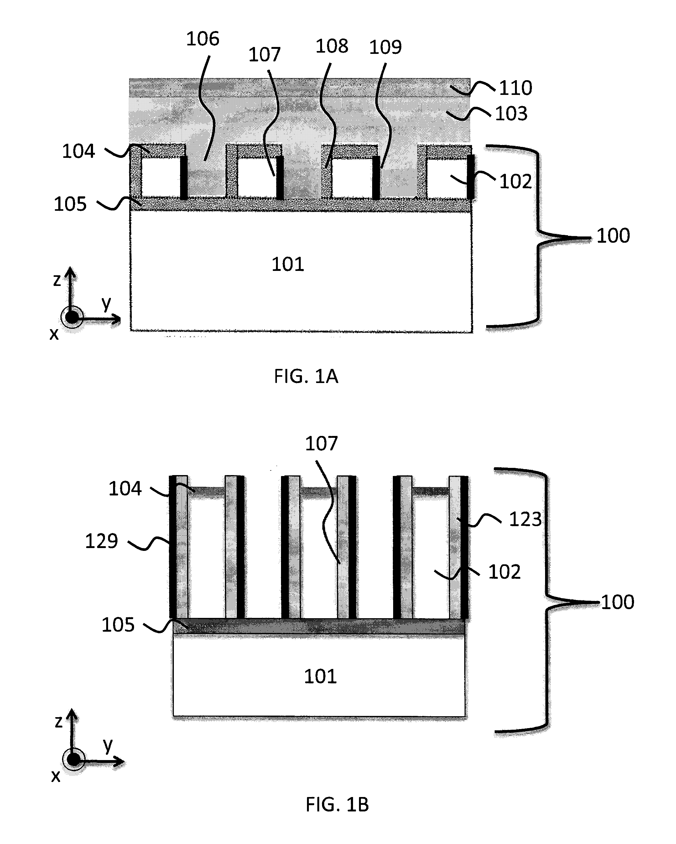
[0036]A method for forming one or more single-crystal Group III-Nitride films with a desired orientation on a patterned substrate is disclosed herein. The substrate is patt...


PUM


Abstract

A method for forming a single crystalline Group-III Nitride film. A substrate is provided, having a first passivation layer, a monocrystalline layer, and a second passivation layer. The substrate is patterned to form a plurality of features with elongated sidewalls having a second crystal orientation. Group-III Nitride films are formed on the elongated sidewalls, but not on the first or second passivation layers. In one embodiment, the dimensions of the patterned features and the film deposition process result in a single crystalline Group-III Nitride film having a third crystal orientation normal to the substrate surface. In another embodiment, the dimensions and orientation of the patterned features and the film deposition process result in a plurality of single crystalline Group-III Nitride films. In other embodiments, additional layers are formed on the Group-III Nitride film or films to form semiconductor devices, for example, a light-emitting diode.

Description

[0001]This Application claims the benefit of and priority to Provisional Application Ser. No. 61 / 413,889 filed Nov. 15, 2010 which is hereby incorporated by reference.BACKGROUND[0002]1. Field[0003]The present invention relates generally to the manufacture of semiconductor devices. In particular, the present invention relates to the formation of a single-crystal Group-III Nitride film with a desired orientation on a patterned substrate.[0004]2. Discussion of Related Art[0005]Single-crystal Group III-Nitride films and related optical and electrical devices are typically grown from planar c-plane sapphire substrates, with the (0001) / c-plane of the Group III-Nitride film oriented in the z-direction, normal to the substrate surface. The c-plane of a Group III-Nitride is polar and has a piezoelectric field; both properties can affect device performance due to energy band distortion, separation of electrons and holes, and reduction of the radiative recombination efficiency. In LED devices,...

Claims


Application Information

Patent Timeline
IPC IPC(8): H01L29/207H01L29/04H01L21/20
CPCC30B25/18C30B29/403H01L21/0237H01L21/02381H01L21/0242H01L21/02433H01L33/007H01L21/02488H01L21/0254H01L21/02639H01L21/02647H01L21/0265H01L21/02458
Inventor SU, JIE
Owner APPLIED MATERIALS INC
Why Eureka
Try Eureka