

Semiconductor memory device
a memory device and semiconductor technology, applied in the direction of digital storage, capacitors, instruments, etc., can solve the problems of difficult to realize a multi-level memory cell in consideration of reading margin, and achieve the effect of increasing the storage capacity of the memory module per unit area
- Summary
- Abstract
- Description
- Claims
- Application Information
AI Technical Summary
Benefits of technology
Problems solved by technology
Method used
Image

Examples
embodiment 1
[0046]In this embodiment, examples of a structure and an operation of a memory cell that is one of semiconductor memory devices will be described with reference to FIGS. 1A and 1B.
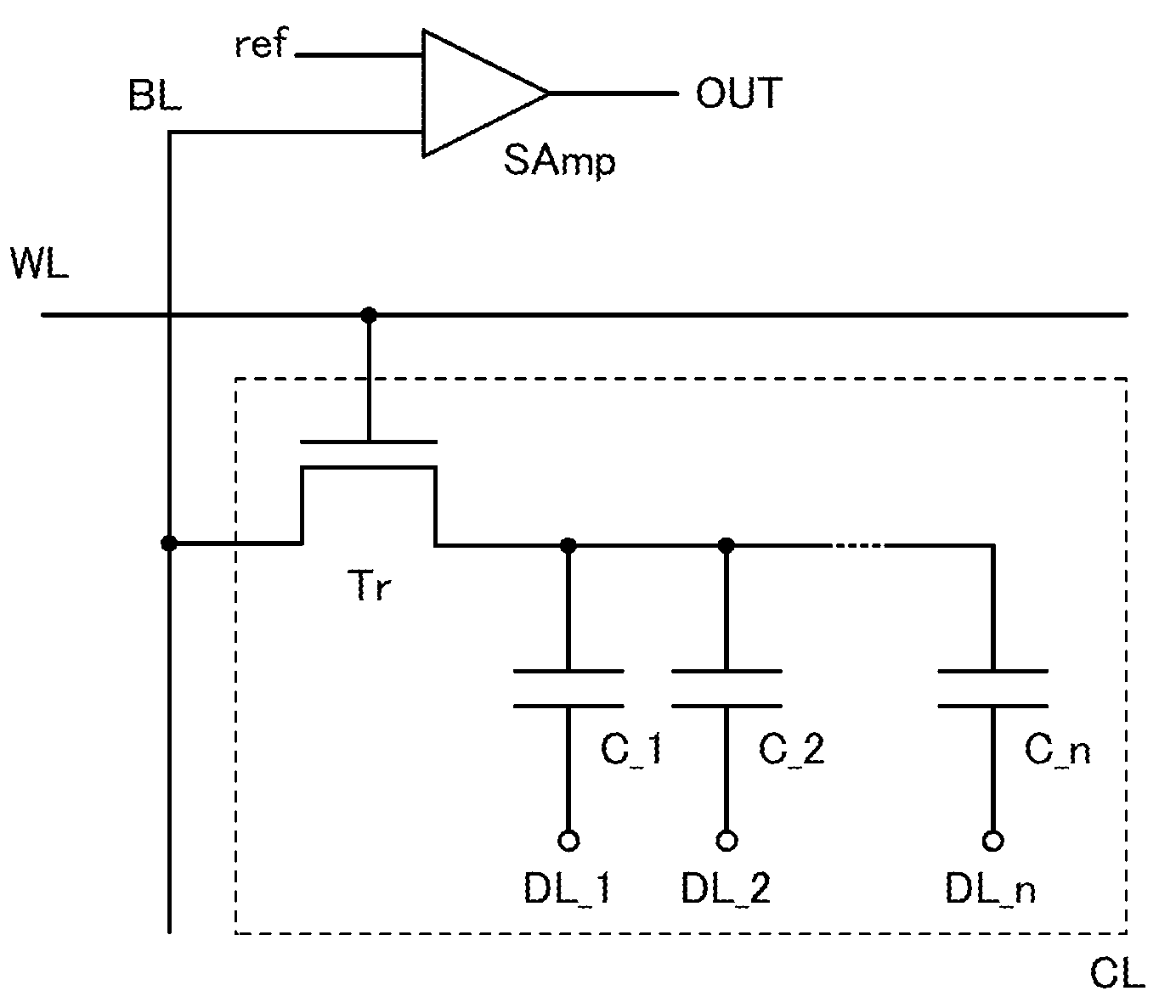
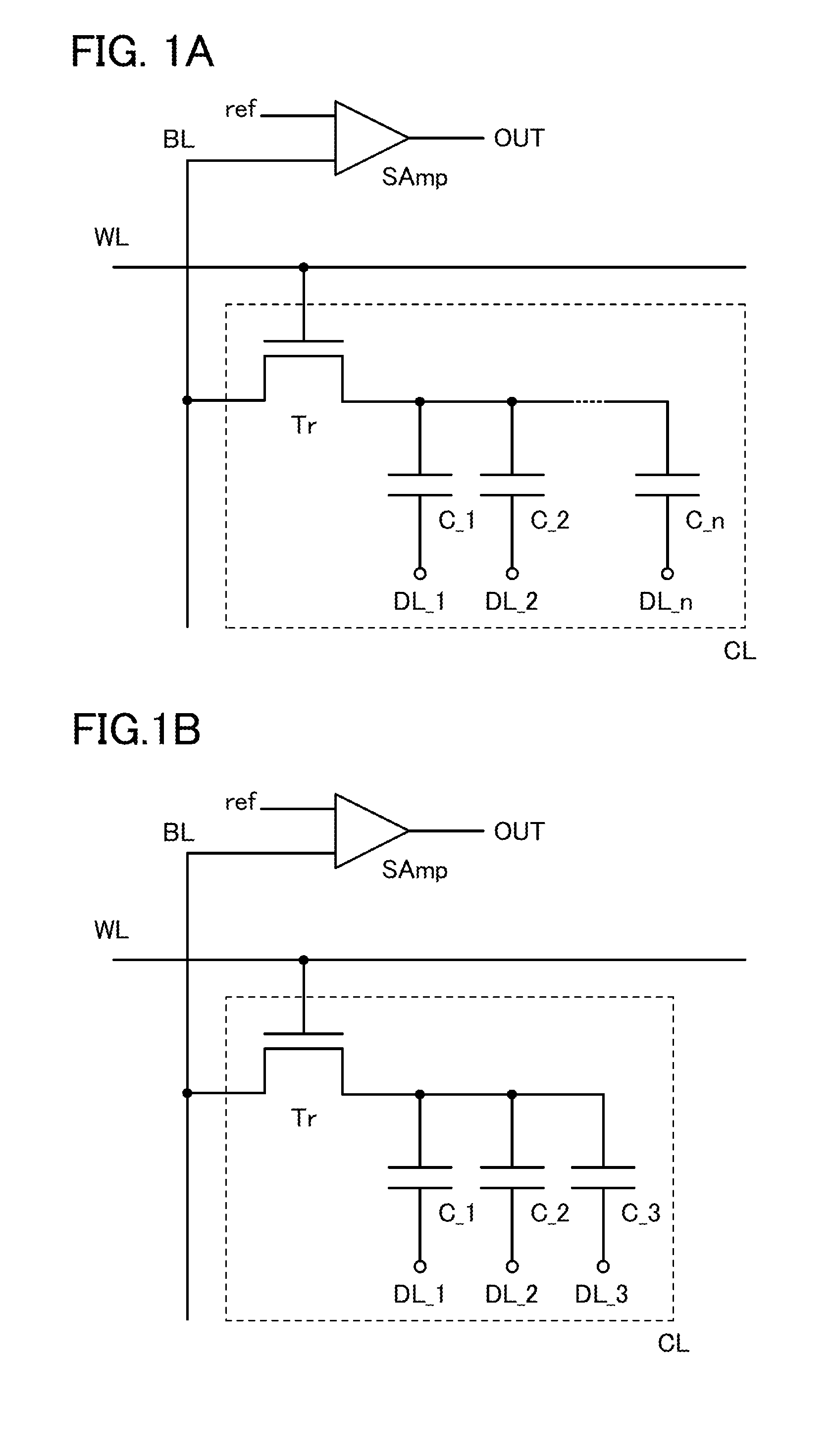
[0047]FIG. 1A is a circuit diagram illustrating a 2n-level memory cell which includes a bit line BL; a word line WL; data lines DL_1 to DL_n; a memory cell CL having a transistor Tr and capacitors C_1 to C_n; and a sense amplifier SAmp.
[0048]A gate of the transistor Tr is connected to the word line WL, one of a source and a drain of the transistor Tr is connected to the bit line BL, the other thereof is connected to one side of each of the capacitors C_1 to C_n, and the other sides of the capacitors C_1 to C_n are connected to the data lines DL_1 to DL_n. For example, the capacitor C_1, the capacitor C_2, and the capacitor C_n are connected to the data line DL_1, the data line DL_2, and the data line DL_n, respectively. The bit line BL is connected to the sense amplifier SAmp.
[0049]As the transistor Tr, a ...
embodiment 2
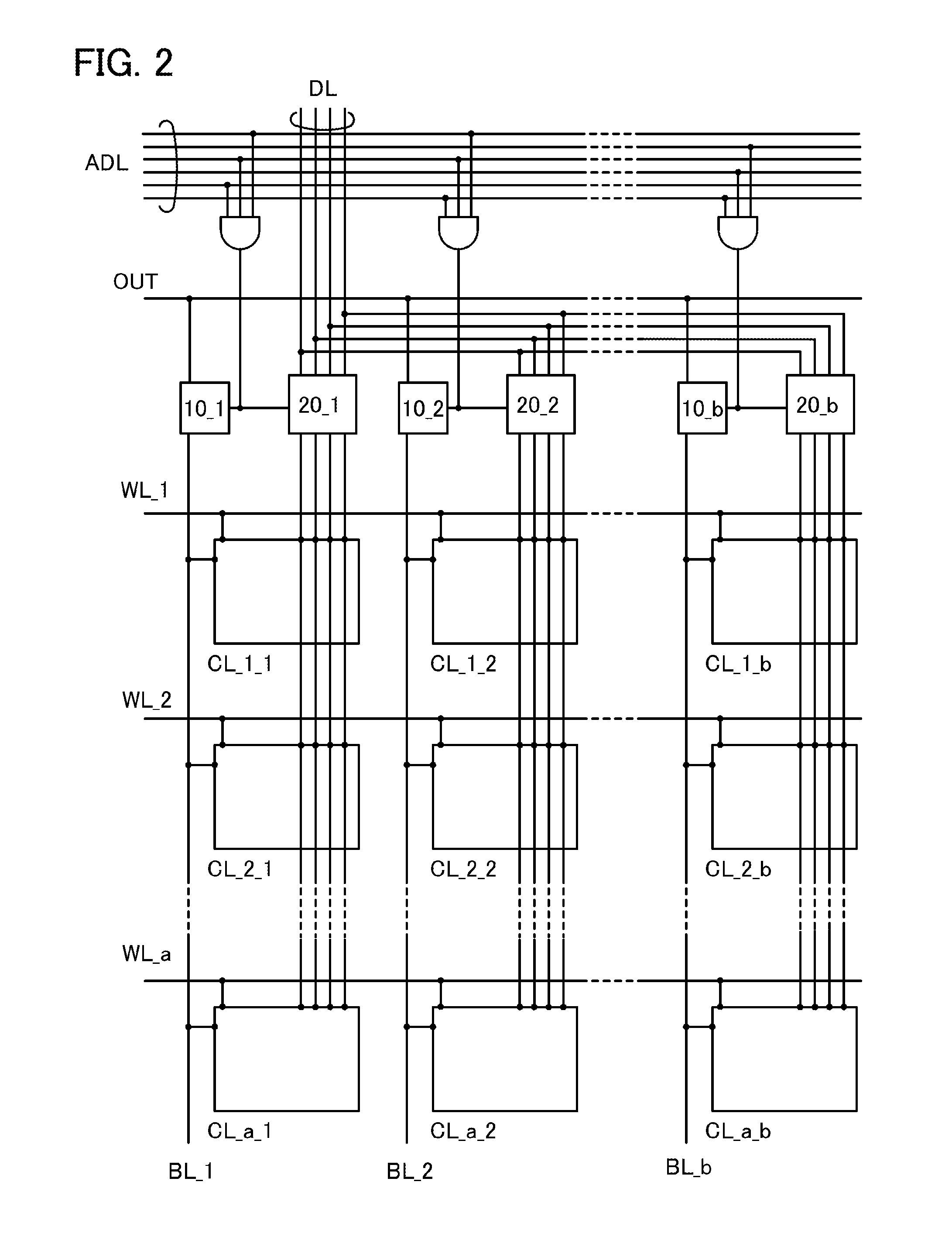
[0065]In this embodiment, a memory module having a rows and b columns using the memory cells described in Embodiment 1 will be described with reference to FIG. 2, as one example of semiconductor memory devices.
[0066]FIG. 2 illustrates a memory module including an address line ADL, a data line DL, bit lines BL_1 to BL_b, word lines WL_1 to WL_a, AND circuits, an output OUT, reading circuits 10_1 to 10—b, switching circuits 20_1 to 20—b, and memory cells CL_1_1 to CL_a_b.
[0067]The address lines ADL are connected to the reading circuits 10_1 to 10—b and the switch circuits 20_1 to 20—b via AND circuits. The data lines DL are each connected to a corresponding capacitor in the memory cells CL_1_1 to CL_a_b via the switch circuits 20_1 to 20—b. The bit line BL_1 is connected to one of a source and a drain of a transistor in each of the memory cells CL_1_1 to CL_a_1 and to the output OUT via the reading circuit 10_1. Similarly, the bit line BL_2 and BL_b are connected to one of a source an...
embodiment 3
[0082]In this embodiment, a memory cell that is one of semiconductor memory devices will be described with reference to FIGS. 3A and 3B.
[0083]FIG. 3A is a cross-sectional view of a semiconductor memory device including a region 300 having a semiconductor substrate 331 and a first insulating film 332; a second insulating film 302 over the region 300; an island-shaped semiconductor film 306 provided over the second insulating film 302; a conductive film 308 and a conductive film 309 which are partially in contact with the semiconductor film 306; a third insulating film 312 provided over the semiconductor film 306, the conductive film 308, and the conductive film 309; a conductive film 304 overlapped with the semiconductor film 306 with the third insulating film 312 interposed therebetween; conductive films 341 to 344 formed with the same layer as the conductive film 304; and a fourth insulating film 316 provided to cover the third insulating film 312, the conductive film 304, and the ...
PUM
 Abstract
Description
Claims
Application Information