Current-Amplifying Transistor Device and Current-Amplifying, Light-Emitting Transistor Device

a technology of current-amplifying transistors and transistors, which is applied in the direction of transistors, thermoelectric devices, nano-informatics, etc., can solve the problems of hardly providing a large current of transistors and the difficulty of shortening the channel length to several micrometers or less, and achieves a large current, high contrast, and high on/off ratio

Active Publication Date: 2012-06-14
DAINICHISEIKA COLOR & CHEM MFG CO LTD +1
View PDF13 Cites 8 Cited by
  • Summary
  • Abstract
  • Description
  • Claims
  • Application Information

AI Technical Summary

Benefits of technology

[0025]Owing to the inclusion of the diode structure in one of the organic semiconductor layers, the current-amplifying transistor device and current-amplifying, light-emitting transistor device according to the present invention can stably provide a current-amplifying effect that enables to perform, at a low voltage, amplification into a large current.
[0026]The current-amplifying transistor device (MBOT) according to the present invention is useful as a drive device for various displays, especially as a drive device for organic EL displays and electronic paper displays which are driven by large-current modulation. Transistor devices for driving these displays are needed to provide a high contrast between an off-state and an on-state so that a higher on / off ratio and suppression of a dark current are required. A low on / off ratio and a large dark current cause a problem such that an organic EL display may emit light even in an off-state. The current-amplifying transistor device according to the present invention is high in on / off ratio and is excellent in large-current modulation characteristics and frequency characteristics in a low voltage range, and therefore, can have high performance as a drive transistor device.
[0027]Further, the current-amplifying transistor device according to the present invention can perform large-current modulation in a low voltage range, can reduce the area occupied by a transistor device in a single pixel, and can provide a display with an improved aperture rate. As a consequence, a high-performance, high-efficiency display can be provided. The current-amplifying transistor device according to the present invention can be fabricated by a vapor deposition process. By forming such current-amplifying transistor devices on a flexible substrate of plastics or the like, a small-size, light-weight display or equipment can be manufactured.
[0028]The current-amplifying, light-emitting transistor device according to the present invention, which has the organic EL device portion formed between the p-type organic semiconductor layer and the n-type organic semiconductor layer in the first organic semiconductor layer or between the second organic semiconductor layer and the collector layer, can be fabricated in a form that an organic light-emitting device and its drive transistor device are combined into a single device. As the organic EL device portion has the organic light-emitting layer, a surface light emission is feasible from the electrode surfaces of such transistor devices. Moreover, no micropatterning is needed for the base electrode unlike the conventional SIT structure, large-current modulation is feasible in a low voltage range, and a high on / off ratio is available. The current-amplifying, light-emitting transistor device is, therefore, excellent as a light-emitting transistor device. Because the current-amplifying, light-emitting transistor device can be fabricated by a vapor deposition process only, the device can be formed on a flexible substrate of plastics or the like. The current-amplifying, light-emitting transistor device can, therefore, be provided as a current-amplifying, light-emitting transistor device of a small-size, light-weight and simple structure. The current-amplifying transistor device and current-amplifying, light-emitting transistor device may hereinafter be called simply “transistor device and light-emitting transistor device” or “MBOT and light-emitting MBOT”.

Problems solved by technology

OFET can hardly provide a large current due to its structure and low mobility.
Practically no report has hence been made about a case in which OFETs are used as drive devices in an organic EL display, said drive devices being current-driven devices that require a large current.
With a patterning technology developed with a view to mass production, however, it is difficult to shorten the channel length to several micrometers or less.

Method used


Image

  • Current-Amplifying Transistor Device and Current-Amplifying, Light-Emitting Transistor Device
  • Current-Amplifying Transistor Device and Current-Amplifying, Light-Emitting Transistor Device
  • Current-Amplifying Transistor Device and Current-Amplifying, Light-Emitting Transistor Device

Examples


example 1

Fabrication of Transistor Device by Diode Structure (C60 / Copper Phthalocyanine)

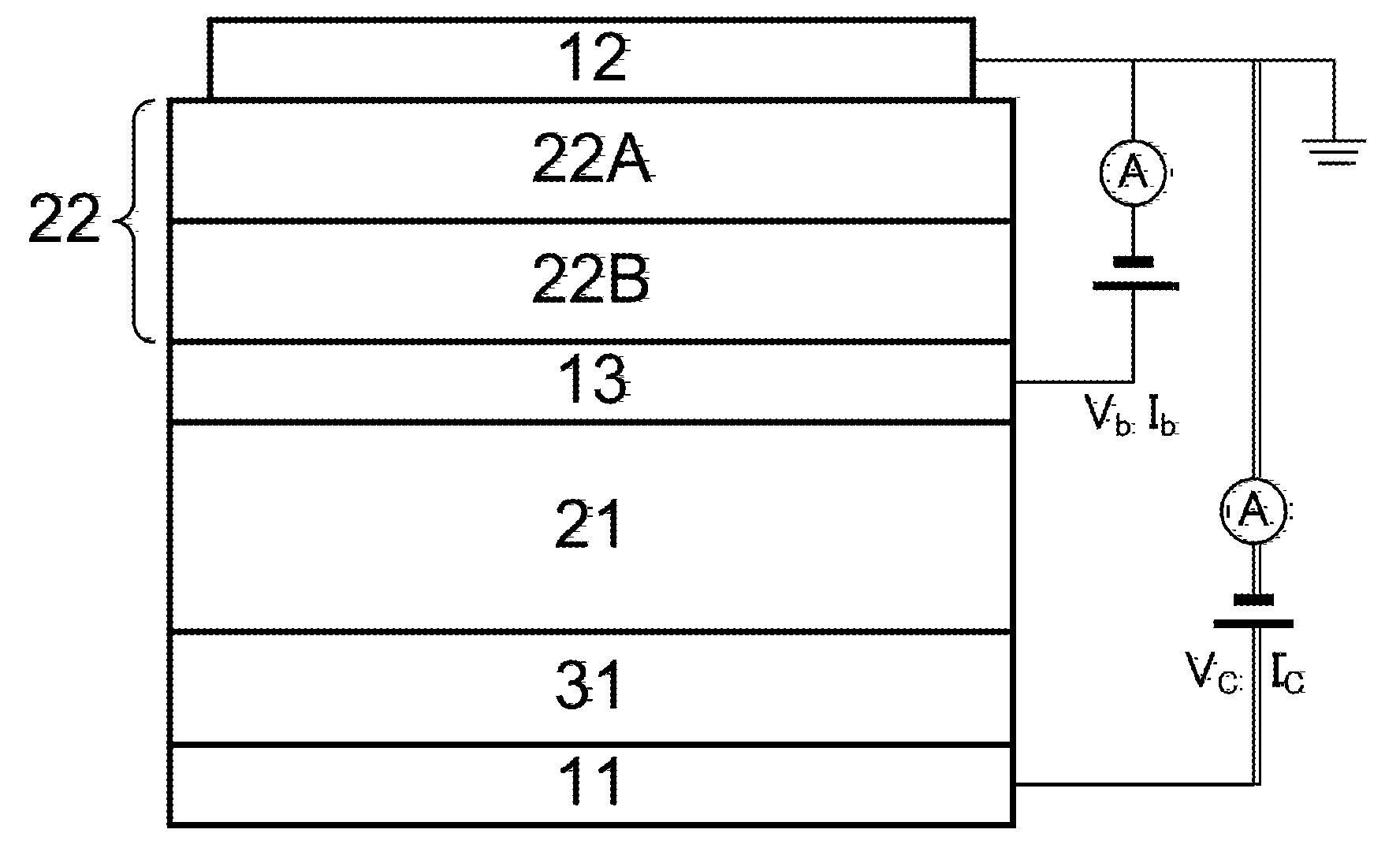
[0101]As illustrated in FIG. 5, an ITO-coated transparent substrate was provided as a collector electrode 11. After an organic semiconductor layer (average thickness: 250 nm) of N,N′-dimethylperylenetetracarboxylic acid diimide (Me-PTCDI, organic semiconductor material) was formed on the collector electrode 11, another organic semiconductor layer (average thickness: 50 nm) of fullerene (C60) was formed to provide a collector layer 21. Subsequent to the formation of an electrode layer (average thickness: 3 nm) of lithium fluoride as an electron injection layer, a base electrode layer (average thickness: 15 nm) of aluminum was stacked to form a base electrode 13. On the base electrode 13, a p-type organic semiconductor layer (average thickness: 30 nm) of copper phthalocyanine and an n-type organic semiconductor layer (average thickness: 50 nm) of fullerene (C60) were stacked in this order by a vacuum deposi...

example 2

Fabrication of Transistor Device by Diode Structure (C60 / Pentacene)

[0103]Similar to Example 1, an ITO-coated transparent substrate was provided as a collector electrode 11. After an organic semiconductor layer (average thickness: 250 nm) of N,N′-dimethylperylenetetracarboxylic acid diimide (Me-PTCDI, organic semiconductor material) was formed on the collector electrode 11, another organic semiconductor layer (average thickness: 50 nm) of fullerene (C60) was formed to provide a collector layer 21. Subsequent to the formation of an electrode layer (average thickness: 3 nm) of lithium fluoride as an electron injection layer on the collector layer 21, a base electrode layer (average thickness: 15 nm) of aluminum was stacked to form a base electrode 13. On the base electrode 13, a p-type organic semiconductor layer (average thickness: 30 nm) of pentacene and an n-type organic semiconductor layer (average thickness: 50 nm) of fullerene (C60) were stacked in this order by a vacuum depositi...

example 3

Fabrication of Light-Emitting Transistor Device by Diode Structure

(B4PYMPM / Pentacene)

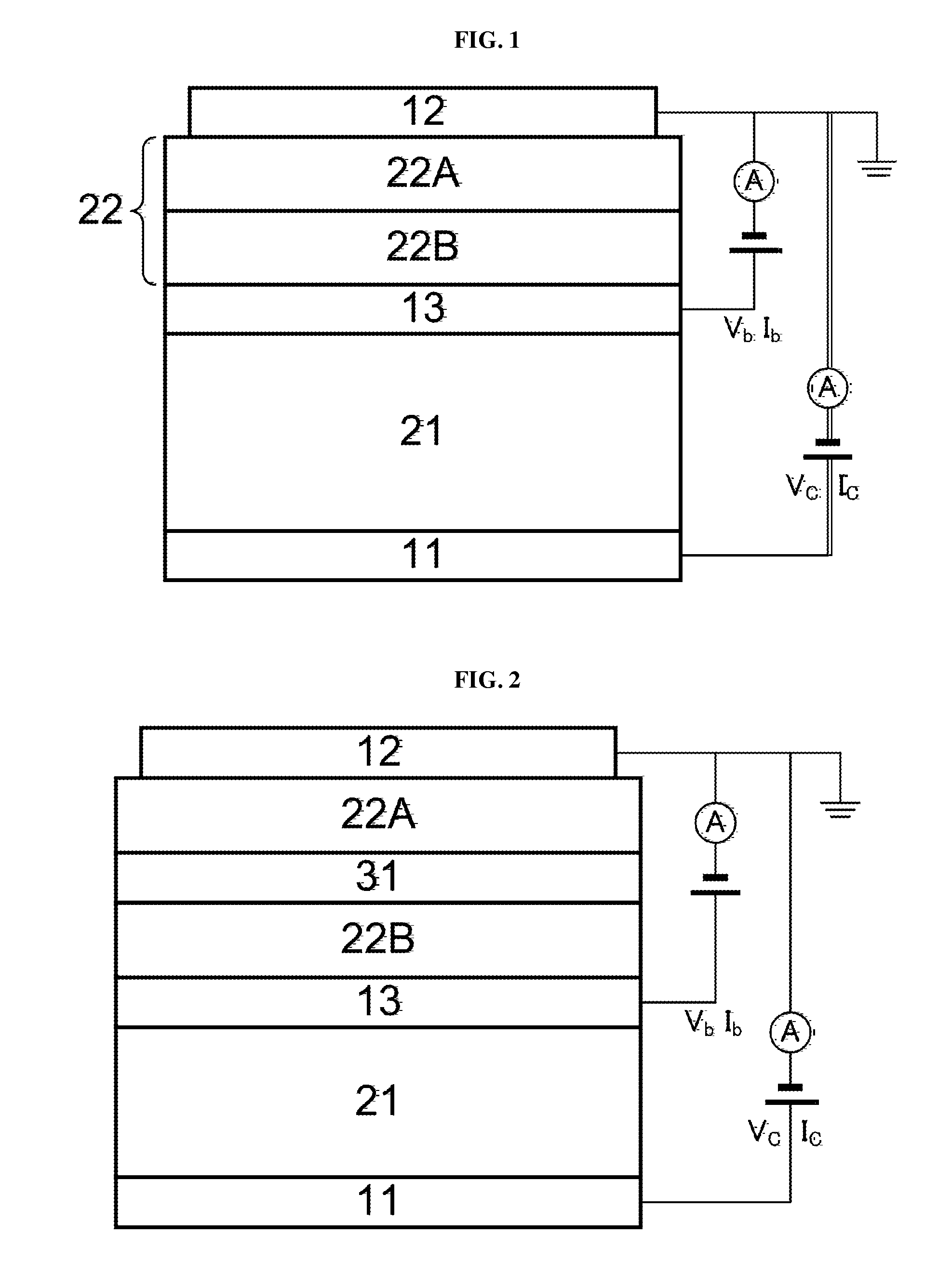
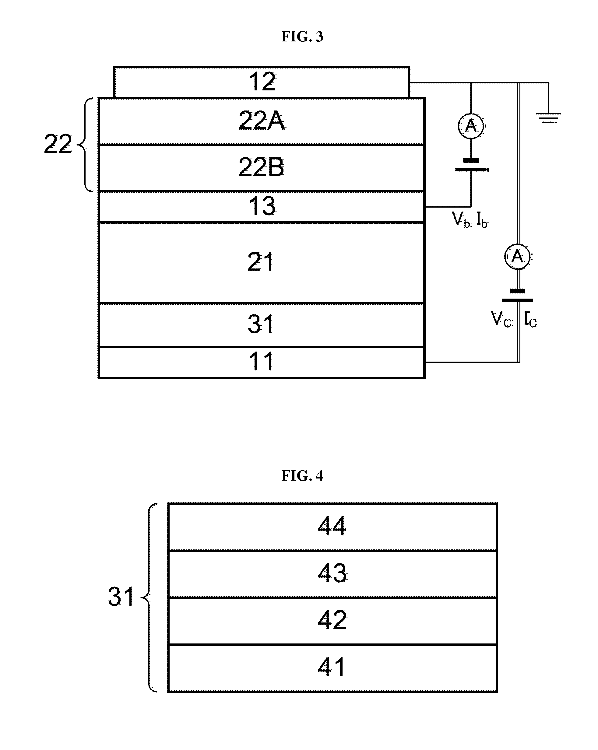
[0105]As depicted in FIG. 6, an ITO-coated transparent substrate was provided as a collector electrode 11. After an organic semiconductor layer (average thickness: 250 nm) of N,N′-dimethylperylenetetracarboxylic acid diimide (Me-PTCDI, organic semiconductor material) was formed on the collector electrode 11, another organic semiconductor layer (average thickness: 50 nm) of fullerene (C60) was formed to provide a collector layer 21 of a stacked structure. Subsequent to the formation of an electrode layer (average thickness: 3 nm) of lithium fluoride as an electron injection layer on the collector layer 21, an electrode layer (average thickness: 15 nm) of aluminum was stacked to form a base electrode 13. On the base electrode 13, a p-type organic semiconductor layer (average thickness: 30 nm) 22B of pentacene, a hole transport layer (average film thickness: 10 nm) of α-NPD [Bis(N-(1-naphthyl)-N-phenyl...


PUM


Abstract

A current-amplifying transistor device is provided, between an emitter electrode and a collector electrode, with two organic semiconductor layers and a sheet-shaped base electrode. One of the organic semiconductor layers is arranged between the emitter electrode and the base collector electrode, and has a diode structure of a p-type organic semiconductor layer and an n-type p-type organic semiconductor layer. A current-amplifying, light-emitting transistor device including the current-amplifying transistor device and an organic EL device portion formed in the current-amplifying transistor device is also disclosed.

Description

TECHNICAL FIELD[0001]This invention relates to a current-amplifying transistor device and a current-amplifying, light-emitting transistor device, each of which has current-amplifying capability, and more specifically, to a current-amplifying transistor device and a current-amplifying, light-emitting transistor device, each of which can perform large-current modulation at a low voltage and is superb in on / off ratio, and therefore, is excellent in driving an organic EL display or the like.BACKGROUND ART[0002]In recent years, flat-screen TV sets and notebook-size personal computers have come into wide use, resulting in increasing demands for liquid crystal displays, organic EL displays, electronic paper displays, and the like. For driving devices in these displays, field-effect transistors (FETs) are used. FETs making use of silicon, an inorganic material, are primarily used these days, but reports have been made about displays that use organic transistor devices for lower manufacturin...

Claims


Application Information

Patent Timeline
Patent Type & Authority Applications(United States)
IPC IPC(8): H01L51/30H05B44/00
CPCH01L51/0504H01L51/0081H01L51/5296H01L51/0046H01L51/0053B82Y10/00H01L51/0067H10K85/211H10K85/621H10K85/654H10K85/324H10K10/00H10K50/30H01L29/73
Inventor NAKAYAMA, KEN-ICHIKIDO, JUNJIPU, YONG-JINSUZUKI, FUMITOOGUMA, NAOMIHIRATA, NAOKI
Owner DAINICHISEIKA COLOR & CHEM MFG CO LTD
Why Eureka
Try Eureka