Plasma processing apparatus, plasma processing method, and non-transitory computer-readable medium

Active Publication Date: 2012-06-21
TOKYO ELECTRON LTD
View PDF54 Cites 22 Cited by
  • Summary
  • Abstract
  • Description
  • Claims
  • Application Information

AI Technical Summary

Benefits of technology

[0014]The present invention is made in view of this problem, and provides a plasma processing apparatus and a plasma processing metho

Problems solved by technology

However, when an etching process is performed by using this type of plasma processing apparatus, an electrode plate of the upper electrode is consumed due to repetitive plasma processing, and accordingly, a temperature of the electrode plate is increased.
However, in future, if a semiconductor device is further miniaturized, it is expected th

Method used


Image

  • Plasma processing apparatus, plasma processing method, and non-transitory computer-readable medium
  • Plasma processing apparatus, plasma processing method, and non-transitory computer-readable medium
  • Plasma processing apparatus, plasma processing method, and non-transitory computer-readable medium

Examples


Example

[0028]Hereinafter, the present invention will be described in detail by explaining exemplary embodiments of the invention with reference to the attached drawings.

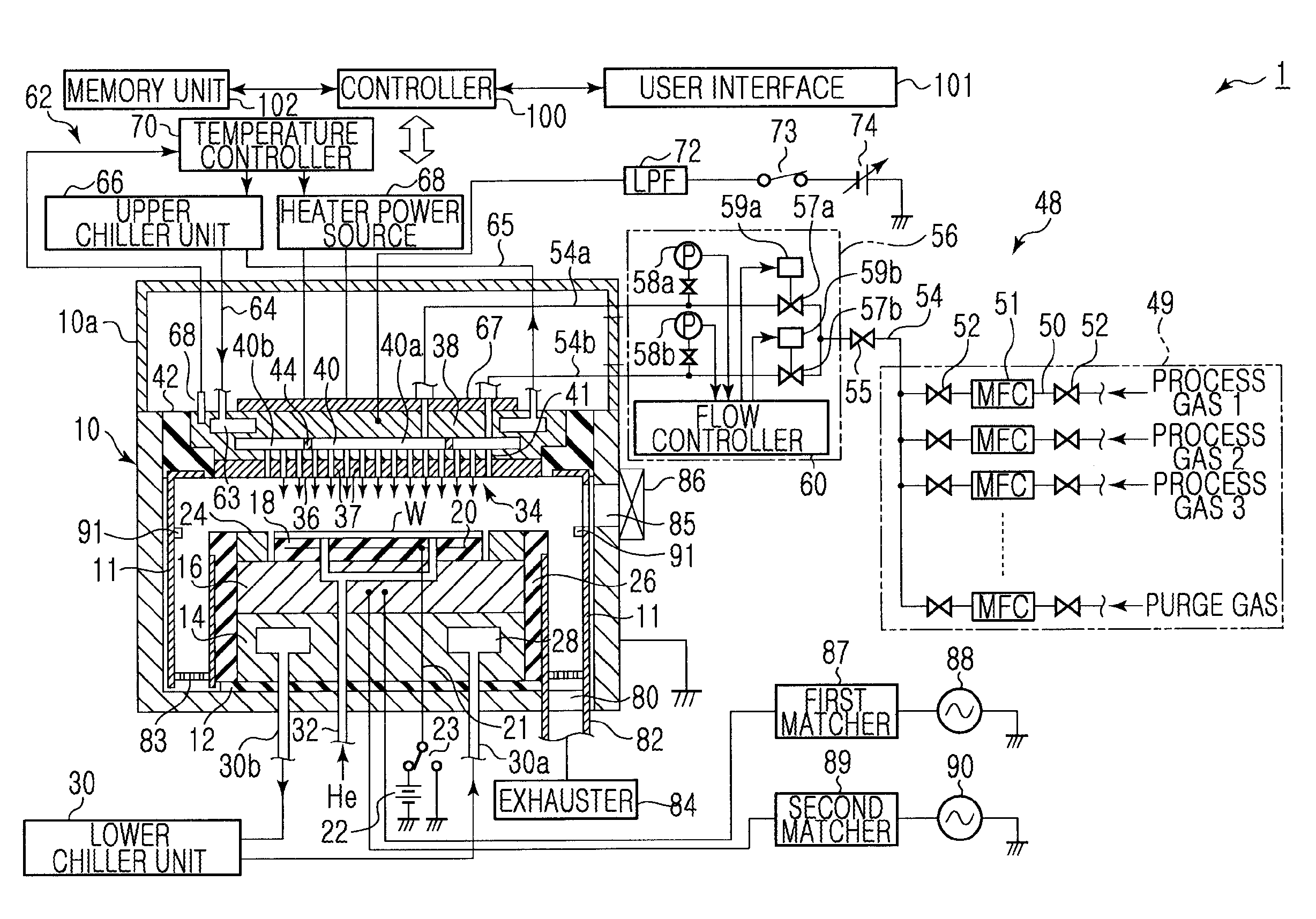
[0029]FIG. 1 is a schematic cross-sectional view of a plasma processing apparatus according to an embodiment of the present invention.

[0030]The plasma processing apparatus 1 is configured as a capacity coupled parallel plate plasma etching apparatus and includes a chamber (a process chamber) 10 having a nearly cylindrical shape and formed of, for example, aluminum of which surface is anodized. The chamber 10 is protectively grounded.

[0031]An insulating plate 12 formed of, for example, ceramics, is disposed at a lower portion of the chamber 10, and a susceptor support 14 having a cylindrical shape is disposed on the insulating plate 12. A susceptor 16 formed of, for example, aluminum, is disposed on the susceptor support 14. The susceptor 16 constitutes a lower electrode, and a semiconductor wafer W, which is a substrate to ...


PUM

PropertyMeasurementUnit
Temperatureaaaaaaaaaa
Pressureaaaaaaaaaa
Flow rateaaaaaaaaaa

Abstract

A plasma processing apparatus includes: a process chamber which accommodates a substrate to be processed; a lower electrode disposed in the process chamber; an upper electrode including an electrode plate that is detachable and discharges a process gas inside the form of shower into the process chamber; a gas supply unit including a central pipe and a edge pipe for supplying the process gas to the upper electrode; a first high frequency power source which applies high frequency power for plasma generation to the lower electrode; pressure indicators which detect pressures inside gas supply pipes; and a controller which measures a degree of consumption of the electrode plate based on the pressures detected by the pressure indicators and calculates a variation in process rate resulting due to the consumption of the electrode plate to adjust process conditions to resolve the variation in process rate.

Description

CROSS-REFERENCE TO RELATED PATENT APPLICATIONS[0001]This application claims the benefits of Japanese Patent Application No. 2010-279294, filed on Dec. 15, 2010 in the Japan Patent Office, and the U.S. Patent Application No. 61 / 429,571, filed on Jan. 4, 2011 in the U.S. Patent and Trademark Office, the disclosures of which are incorporated herein in its entirety by reference.BACKGROUND OF THE INVENTION[0002]1. Field of the Invention[0003]The present invention relates to a plasma processing apparatus for performing plasma processing such as plasma etching, a plasma processing method, and a non-transitory computer-readable medium storing a program for executing the plasma processing method.[0004]2. Description of the Related Art[0005]For example, in a process of manufacturing a semiconductor device, plasma processing, e.g., etching or chemical vapor deposition (CVD), is widely performed on a semiconductor wafer which is a substrate to be processed.[0006]Among various plasma processing ...

Claims


Application Information

Patent Timeline
IPC IPC(8): B23K10/00
CPCG03F7/427H01L21/31138H01J37/32935H01J37/32816H01J37/32091H01L21/205H01L21/3065
Inventor MATSUURA, SHIN
Owner TOKYO ELECTRON LTD
Why Eureka
Try Eureka