
Etchant, display device and method for manufacturing display device using the same

a display device and display device technology, applied in non-linear optics, instruments, chemistry apparatuses and processes, etc., can solve the problems of deterioration of the profile of the thick copper wiring, increase the size of the display device, increase the thickness of the copper wiring, etc., and achieve the effect of improving the etching characteristics of the thick copper layer

Active Publication Date: 2012-06-21
SAMSUNG DISPLAY CO LTD +1
View PDF5 Cites 19 Cited by
  • Summary
  • Abstract
  • Description
  • Claims
  • Application Information

AI Technical Summary

Benefits of technology

[0009]In an embodiment, an etchant is provided, having an advantage of showing improved etching characteristics during an etching process to form thick copper wiring.
[0024]According to exemplary embodiments, etching characteristics of a thick copper layer can be improved by using the copper-titanium etchant or the copper etchant.

Problems solved by technology

Increasing the size of display devices also increases the thickness of the copper wiring, which in turn may cause a deterioration of profile in the thick copper wiring during the etching process.

Method used


Image

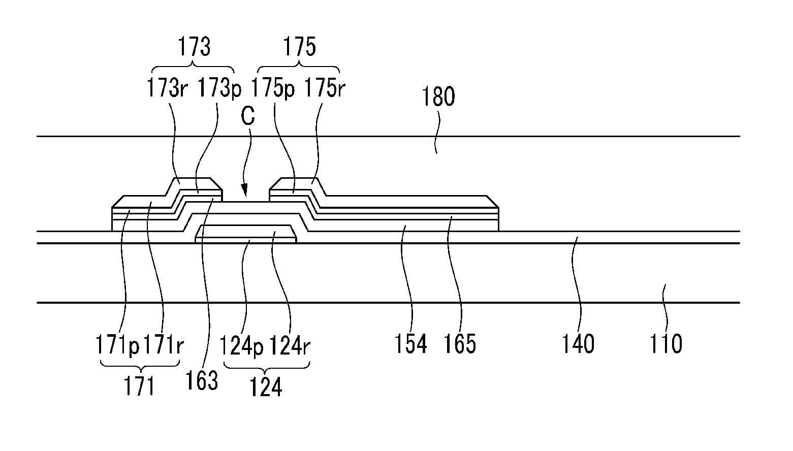
  • Etchant, display device and method for manufacturing display device using the same
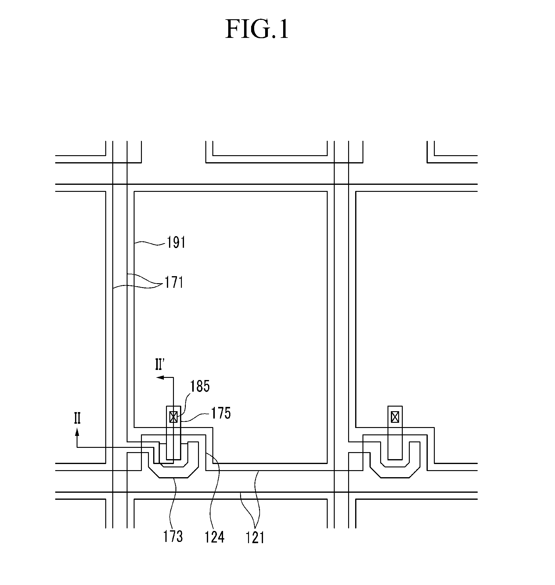
  • Etchant, display device and method for manufacturing display device using the same
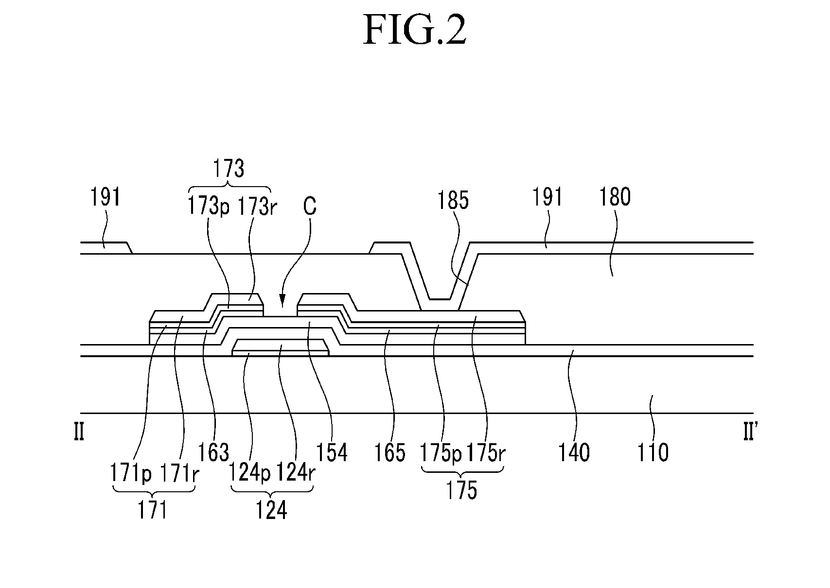
  • Etchant, display device and method for manufacturing display device using the same

Examples


example 1

[0062]As shown in Table 1, 180 kg of a copper-titanium etchant that contains 10 wt % of ammonium persulfate, 0.5 wt % of ammonium bifluoride, 3 wt % of nitric acid, 1 wt % of 5-aminotetrazole, 3 wt % of ammonium acetate, 5 wt % of acetic acid, 2 wt % of p-toluenesulfonic acid and water was prepared.

experimental example 1

Evaluation of Etching Characteristics

[0064]A SiNx layer is deposited on a glass substrate by PECVD, a titanium layer having a thickness of 300 angstrom (Å) is laminated onto the SiNx layer, and a copper layer having a thickness of 15000 angstrom (Å) is laminated on the titanium layer. A photoresist was applied to the copper surface and patterned, and the substrate having the predetermined photoresist pattern on the copper layer was cut using a diamond blade to prepare samples of 550×650 mm.

[0065]The copper-titanium etchants of Example 1 and Comparative Example 1 were loaded into a spray type etching test apparatus, and heated to a temperature in excess of 25° C. Thereafter, when the etchant temperature reached 30±0.1° C., an etching process was performed to form wiring features. A total etching time was performed to achieve 40% of the standard for end-point detection (“EPD”). The sample was loaded, and the spray etching was performed. When the etching to open the wiring test feature...

experimental example 2

Evaluation of Storage Characteristics

[0066]The copper-titanium etchants of Example 1 and Comparative Example 1 were prepared in a quantity sufficient to perform a reference etch, and the remaining etchant for each was stored at 25° C. for a scheduled storage test date of 5 days. After the scheduled date, an etching test was again performed using the aged etchants of Example 1 and Comparative Example 1 under the same conditions used for the reference etch. The results were then compared with the reference etch test results. The results are shown in Table 2.


PUM

PropertyMeasurementUnit
wt %aaaaaaaaaa
wt %aaaaaaaaaa
thicknessaaaaaaaaaa

Abstract

An etchant includes: 5 to 20 wt % of persulfate, 1 to 10 wt % of at least one compound of an inorganic acid, an inorganic acid salt, or a mixture thereof, 0.3 to 5 wt % of a cyclic amine compound, 1 to 10 wt % of at least one compound of an organic acid, an organic acid salt, or a mixture thereof, 0.1 to 5 wt % of p-toluenesulfonic acid, and water, based on the total weight of the etchant. A copper-titanium etchant further includes 0.01 to 2 wt % of a fluoride-containing compound. A method of forming a display device using the etchant, and a display device, are also disclosed.

Description

[0001]This application claims priority to Korean Patent Application No. 10-2010-0128314 filed on Dec. 15, 2010, and all the benefits accruing therefrom under 35 U.S.C. 119, the contents of which in their entirety are herein incorporated by reference.BACKGROUND OF THE INVENTION[0002](1) Field of the Invention[0003]The present invention relates to an etchant, a display device using the same and a method for manufacturing the display device.[0004](2) Description of the Related Art[0005]In general, thin film transistor (“TFT”) array panels are used as a circuit board for independently driving each pixel in liquid crystal displays, organic electro luminescence (“EL”) display devices, etc. The thin film transistor array panel has a scanning signal wire that transfers a scanning signal on a gate wire, and an image signal line that transfers an image signal on a data wire, and further includes a thin film transistor that is connected to the gate wire and the data wire, and a pixel electrode...

Claims


Application Information

Patent Timeline
Patent Type & Authority Applications(United States)
IPC IPC(8): H01L33/16C09K13/08C09K13/06
CPCH01L27/124H01L27/1259H01L27/127H01L21/32134H01L29/41733C23F1/02C23F1/18C23F1/26C09K13/00C09K13/06C09K13/08G02F1/13H10K99/00
Inventor PARK, HONG-SICKLEE, WANG-WOOKIM, SANG-TAELEE, JOON-WOOPARK, YOUNG-CHULJIN, YOUNG-JUNKANG, KYONG-MINYOON, YOUNG-JINLEE, SUCK-JUNKWON, O-BYOUNGYU, IN-HOJANG, SANG-HOONLIM, MIN-KIKIM, DONG-KI
Owner SAMSUNG DISPLAY CO LTD
Learn More