

Method for manufacturing liquid crystal display element
a technology of liquid crystal display element and manufacturing method, which is applied in the direction of polarising element, instruments, other domestic articles, etc., can solve the problems of increasing the risk of film breakage, and preventing reliably the effect of pressure-sensitive adhesive layer cutting
- Summary
- Abstract
- Description
- Claims
- Application Information
AI Technical Summary
Benefits of technology
Problems solved by technology
Method used
Image

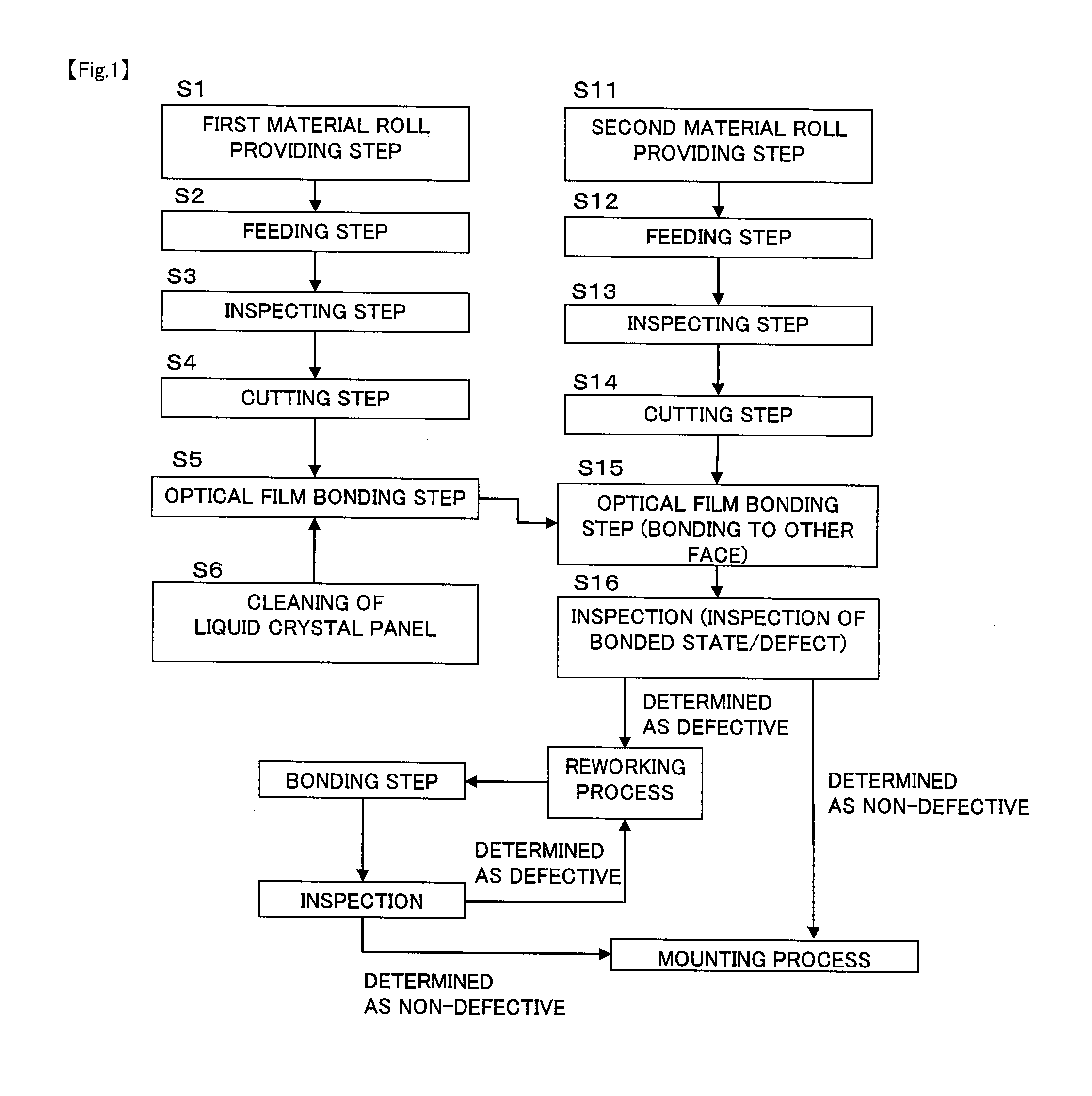
Examples
example 1
[0101]The sheet material used was a laminate of an optical film serving as a polarizing plate, a carrier film (PET, 38 μm in thickness, 202 MPa in breaking strength), and a surface protecting film (PET, 38 μm in thickness) with pressure-sensitive adhesive layers (acrylic pressure-sensitive adhesive, each 23 μm in thickness) interposed therebetween, respectively. The optical film was composed of a polarizer (an oriented iodine-containing PVA film, 28 μm in thickness) and polarizer-protecting films (triacetylcellulose films, each 80 μm in thickness) placed on both sides of the polarizer with an adhesive layer (PVA-based adhesive, 80 nm in thickness) interposed therebetween.
[0102]A long piece of the sheet material (400 mm in width) was cut at predetermined intervals to different average depths in the range from −15 μm to +35 μm using a cutter having a flat-surface mount and a cutting mechanism in which the edge of a cutter knife blade was allowed to slide (at a moving speed of 350 mm / s...
example 2
[0104]Cutting and evaluation were performed under the same conditions as those in Example 1, except that the thickness of the carrier film was changed to 25 μm and that the average cut depth was changed in the range from −12 μm to +20 μm in response to the change in thickness. The results are shown in Table 2.
TABLE 2Degradationin theappearancePercentagePercentageHeight ofAverage cutof bondedof cutof uncutuncutdepthmaterialportionportionportion+20 μmbroken18%0%+15 μmbroken46%0% +4 μm∘84%2%1 μm 0 μmΔ41%13% 4 μm −4 μmx10%78% 9 μm−12 μmx 0%100% 18 μm
[0105]The results in Table 2 show that when the percentage of the cut portion was 60% or more, breaking was not observed. When the percentage of the uncut portion was 10% or less and when the height of the uncut portion was 3 μm or less, the appearance of the bonded material was evaluated as “o” with respect to degradation.
example 3
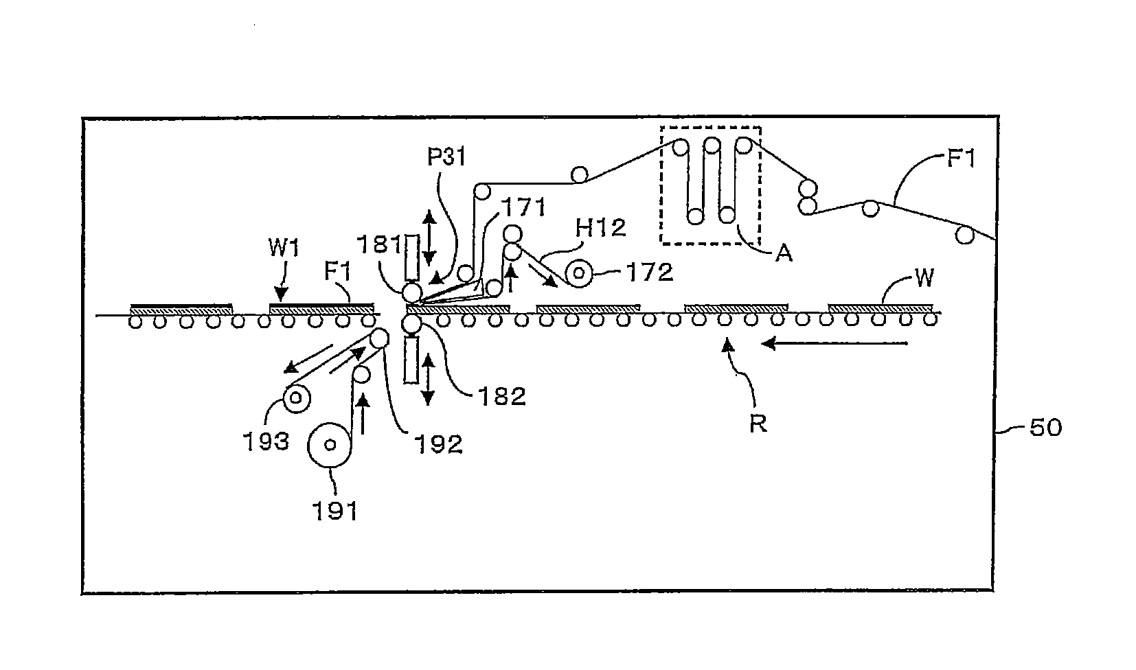
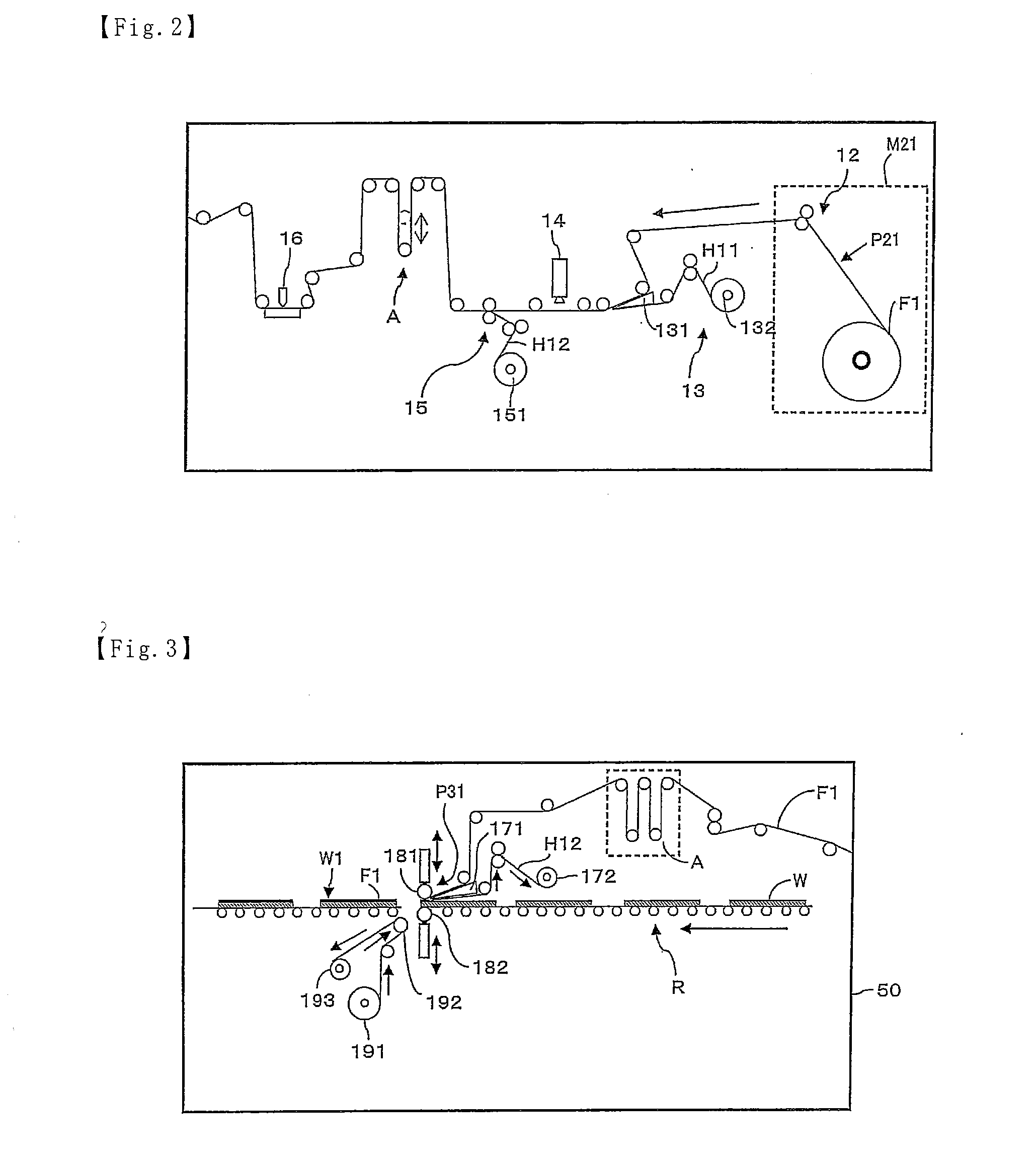
[0106]The optical film pieces resulting from the cutting in Examples 1 and 2 were used. A liquid crystal panel and each optical film piece were bonded together using the bonding apparatus shown in FIG. 3 (the radius of curvature of the edge of the peeling bar used to peel off the carrier film was 1.5 mm; the turning angle was 170° (the interior angle was 10°); the tensile force was 0.15 N / mm), which was provided continuously to the apparatus shown in FIG. 2. In this process, evaluation was performed as described above. The results of the evaluation are shown in Table 3.
TABLE 3Length ofcompletelyThickness ofEvaluationEvaluationcut portionboth endof breakageof breakageFilmat both endportionsduringduringthicknessportionsleft uncutcarryingpeeling-off38 μmright 0 mm,right 22,not brokennot brokenleft 0 mmleft 2138 μmright 0 mm,right 20,not brokennot brokenleft 0 mmleft 2525 μmright 0 mm,right 13,not brokennot brokenleft 0 mmleft 1238 μmright 0 mm,right 8,not brokenbrokenleft 0 mmleft 538 ...
PUM
| Property | Measurement | Unit |
|---|---|---|
| thickness | aaaaa | aaaaa |
| thickness | aaaaa | aaaaa |
| thickness | aaaaa | aaaaa |
Abstract
Description
Claims
Application Information