Piezoelectric vibration device, method of manufacturing the same, and method of adjusting resonant frequency

a technology of piezoelectric vibration and piezoelectric, which is applied in the direction of device details, device material selection, and device details, etc., can solve the problems of reducing the production lot, and reducing the production yield, so as to prevent the increase in the surface roughness of the surface acoustic wave element and the structural breakage. , to increase the wave velocity

Inactive Publication Date: 2012-02-16
SEIKO EPSON CORP
View PDF10 Cites 5 Cited by
  • Summary
  • Abstract
  • Description
  • Claims
  • Application Information

AI Technical Summary

Benefits of technology

[0013]An advantage of some aspects of the invention is to provide a piezoelectric vibration device arranged to be capable of raising the resonant frequency while preventing the increase in the surface roughness and the structural breakage, a method of manufacturing the piezoelectric vibration device, and a method of adjusting the resonant frequency.
[0016]According to such a method, the resonant frequency of the surface acoustic wave element can be raised using the relationship of the formula 1. There is no need for scraping away the surface of the surface acoustic wave element using a physical or chemical measure such as sputtering-out by ion beam irradiation on the surface of the surface acoustic wave element or etching by gas plasma when adjusting the resonant frequency. Therefore, it is possible to raise the resonant frequency while preventing the increase in the surface roughness of the surface acoustic wave element and the structural breakage.
[0020]By forming the functional film having the “high Young's modulus” and the “low density” on the surface of the surface acoustic wave element, it is possible to develop the frequency rise due to the elastic modulus rise while suppressing the influence of the frequency drop due to the mass attachment effect to thereby raise the resonant frequency.
[0025]Further, in the method of manufacturing a piezoelectric vibration device described above, it is also possible that there is further provided with: forming, prior to the measuring a resonant frequency, one of an insulating film, a water-repellent film, and an oil-repellent film on a surface of the surface acoustic wave element, and in the measuring a resonant frequency, the resonant frequency is measured in a condition in which one of the insulating film, the water-repellent film, and the oil-repellent film is formed, and in the forming a functional film, the functional film is formed on one of the insulating film, the water-repellent film, and the oil-repellent film. According to such a method, the electrical short between the excitation electrodes of the surface acoustic wave element, the corrosion or the contamination due to moisture or an organic component can be prevented. Further, since the sputtering-out by the ion beam irradiation, the etching by the gas plasma, or the like for raising the resonant frequency of the surface acoustic, element is not performed, the structural breakage can also be prevented with respect to this film. It should be noted that “one of the insulating film, the water-repellent film, and the oil-repellent film” corresponds to, for example, a thin film 5 described later.
[0026]Another aspect of the invention is directed to a piezoelectric vibration device having a surface acoustic wave element including a functional film formed on a surface of the surface acoustic wave element, wherein the functional film has a function of increasing a velocity of a wave. According to such a configuration, it is possible to raise the resonant frequency while preventing the increase in the surface roughness of the surface acoustic wave element and the structural breakage.
[0032]Still another aspect of the invention is directed to a method of adjusting a resonant frequency of a surface acoustic wave element, including raising the resonant frequency by forming a functional film adapted to increase a velocity of a wave on a surface of the surface acoustic wave element. According to such a method, it is possible to raise the resonant frequency while preventing the increase in the surface roughness of the surface acoustic wave element and the structural breakage.

Problems solved by technology

However, since each SAW element includes production tolerance (e.g., tolerance in the manufacturing dimension or mass of the piezoelectric body, and tolerance in the manufacturing dimension or mass of the electrode), it results that a deviation from the design value is caused in the resonant frequency of each SAW element.
Incidentally, according to the first method described above, since the frequency can only be lowered, if the frequency is lowered beyond the desired value by chance, it is not possible to restore the production lot, which causes degradation of production yield.
Further, according to the second method, it results that the part of the SAW element is destroyed in the elementary sense.
Therefore, it results that the roughness of the excitation electrode surface of the SAW element and the quartz crystal surface is increased, and thus, the possibility of deterioration of the frequency characteristics arises.
In this case, due to the ion beam irradiation or the plasma etching on the thin film having been formed while taking the trouble, there is a possibility that the thin film causes structural breakage, and fails to sufficiently exert the insulating property, the water repellency, the oil repellency, and so on.
However, as described above, in the case of raising the frequency, there still remains the problem of, for example, the deterioration of the frequency characteristics due to the increase in the surface roughness, and the degradation of the insulating property, the water repellency, and the oil repellency due to the structural breakage.

Method used


Image

  • Piezoelectric vibration device, method of manufacturing the same, and method of adjusting resonant frequency
  • Piezoelectric vibration device, method of manufacturing the same, and method of adjusting resonant frequency
  • Piezoelectric vibration device, method of manufacturing the same, and method of adjusting resonant frequency

Examples


Embodiment Construction

[0045]An embodiment of the invention will hereinafter be explained with reference to the accompanying drawings. It should be noted that in the drawings hereinafter explained, the parts having the same configurations are provided with the same reference numerals, and duplicated explanations therefor will be omitted.

1. Regarding Configuration Example of Piezoelectric Vibration Device

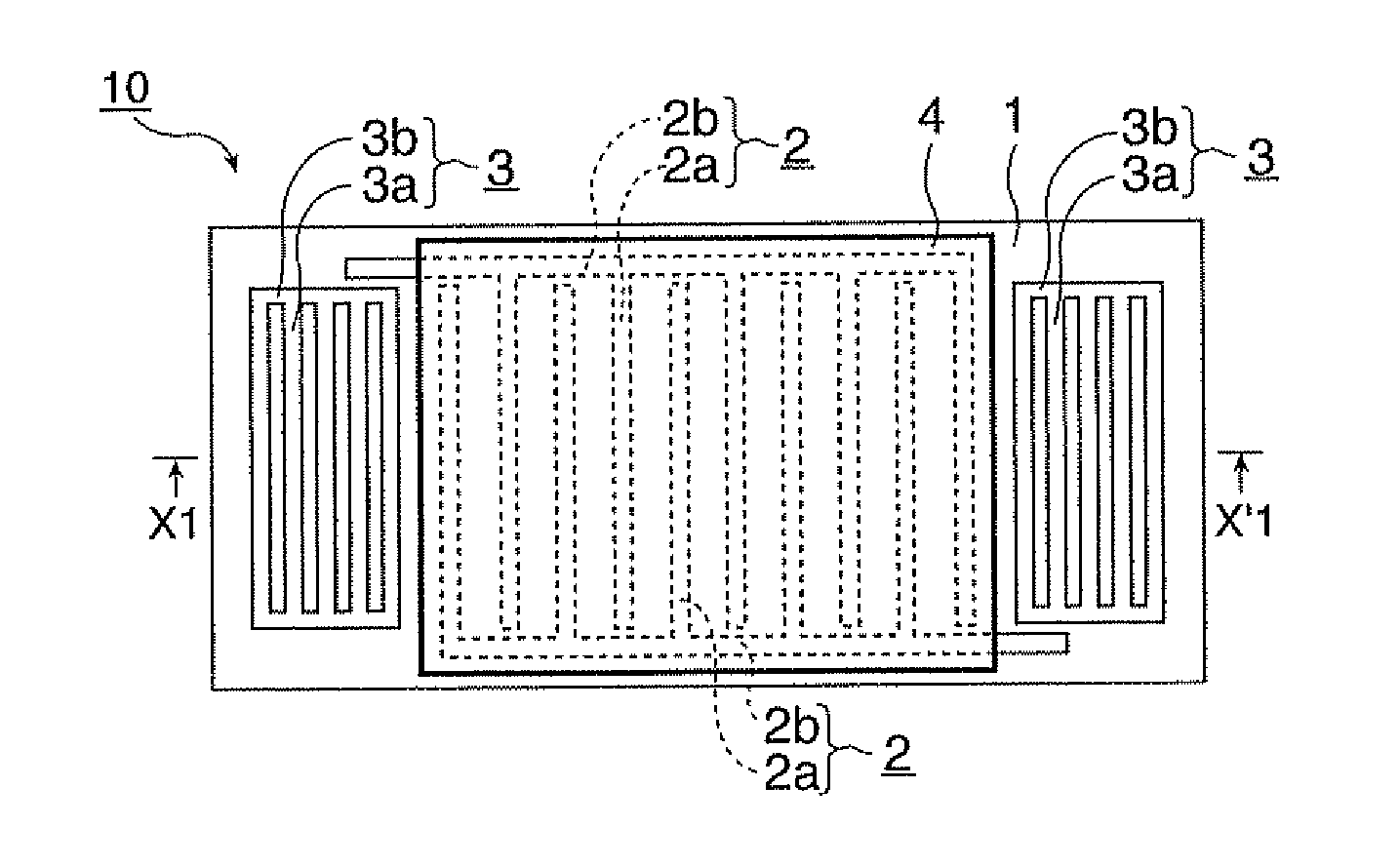
[0046]FIGS. 1A and 1B are diagrams showing a configuration example of a surface acoustic wave (i.e., SAW) element 10 according to the embodiment of the invention, wherein FIG. 1A is a plan view, and FIG. 1B is a cross-sectional view obtained by cutting the plan view of FIG. 1A along a line X1-X′1.

[0047]As shown in FIGS. 1A and 1B, the SAW element 10 is formed on the surface of the piezoelectric body 1, and is provided with excitation electrodes 2 and reflectors 3 formed on the surface of the piezoelectric body 1, and a functional film 4 formed on the surface of the piezoelectric body 1 so as to cover the e...


PUM

PropertyMeasurementUnit
Young's modulusaaaaaaaaaa

Abstract

A method of manufacturing a piezoelectric vibration device having a surface acoustic wave element includes a step of forming a functional film adapted to increase a velocity of a wave on a surface of the surface acoustic wave element. Further, the Young's modulus of the functional film is higher than the Young's modulus of each of the excitation electrode and the piezoelectric body, and the density of the functional film is lower than the density of each of the excitation electrode and the piezoelectric body. Thus, it is possible to develop the frequency rise due to the elastic modulus rise while suppressing the influence of the frequency drop due to the mass attachment effect to thereby raise the resonant frequency of the surface acoustic wave element.

Description

[0001]The entire disclosure of Japanese Patent Application No. 2010-181805, filed Aug. 16, 2010 and Japanese Patent Application No. 2011-093343, filed Apr. 19, 2011 are expressly incorporated by reference herein.BACKGROUND[0002]1. Technical Field[0003]The present invention relates to a piezoelectric vibration device, a method of manufacturing the piezoelectric vibration device, and a method of adjusting the resonant frequency.[0004]2. Related Art[0005]In various electronic devices such as communication devices, computers, or mobile devices, there is used a piezoelectric vibration device having a surface acoustic wave (SAW) element as an electronic component such as a vibrator, an oscillator, or a filter. The piezoelectric vibration devices assume the role of vibrator / filter for transmitting / receiving sync signals and only the signals with appropriate frequencies of electronic devices, and therefore, the accuracy of the SAW resonant frequency to the base thereof is important.[0006]Ho...

Claims


Application Information

Patent Timeline
Patent Type & Authority Applications(United States)
IPC IPC(8): H01L41/04H04R17/00H01L41/09H01L41/18H01L41/22H01L41/23H01L41/253H03H3/08H03H9/145H03H9/25
CPCH03H3/10H03H9/25H03H2003/0442Y10T29/42
Inventor WADA, MITSUHIROKATO, TATSUSHITANAKA, SATORU
Owner SEIKO EPSON CORP
Why Eureka
Try Eureka