Method of manufacturing a light emission device based on light emitting diodes

a technology of light-emitting diodes and manufacturing methods, which is applied in the direction of solid-state devices, basic electric elements, electric devices, etc., can solve the problems of low efficiency of such diodes, reduced service life of leds, and complex manufacturing of leds, etc., to achieve improved heat dissipation characteristics, improved efficiency, and high brightness

Inactive Publication Date: 2012-06-28
COMMISSARIAT A LENERGIE ATOMIQUE ET AUX ENERGIES ALTERNATIVES
View PDF11 Cites 53 Cited by
  • Summary
  • Abstract
  • Description
  • Claims
  • Application Information

AI Technical Summary

Benefits of technology

[0010]An aim of the present invention is to solve the aforementioned problem by proposing a simple method of manufacturing a light emi

Problems solved by technology

The manufacture of this type of LED, however, remains complex and expensive since it requires very many steps, in particular steps of thinning and/or shrinkage of the epitaxial growth substrate and, where applicable, a step of attaching the LEDs to a PCB.
In doing this, not only is the efficiency of such diodes low, but the service life thereof is substantially shortened if they suffer significant heating.
Problems of thermal dissipation are thus posed, all the more so when a high brightness of the lighting system, and therefore a large number of diodes, is required.
In fact, thermal dissipation remains the main reason why this ty

Method used


Image

  • Method of manufacturing a light emission device based on light emitting diodes
  • Method of manufacturing a light emission device based on light emitting diodes
  • Method of manufacturing a light emission device based on light emitting diodes

Examples


Embodiment Construction

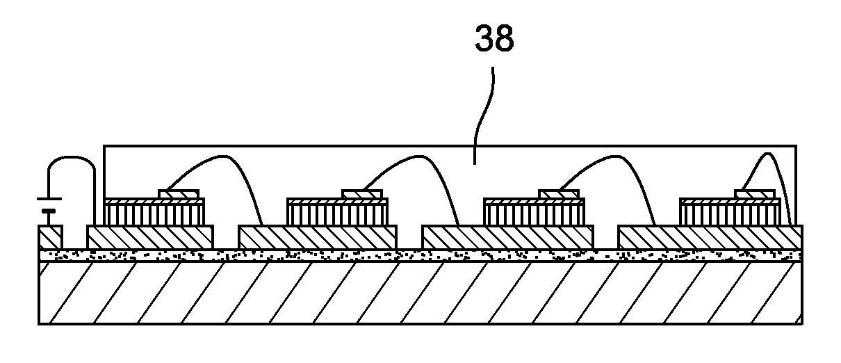
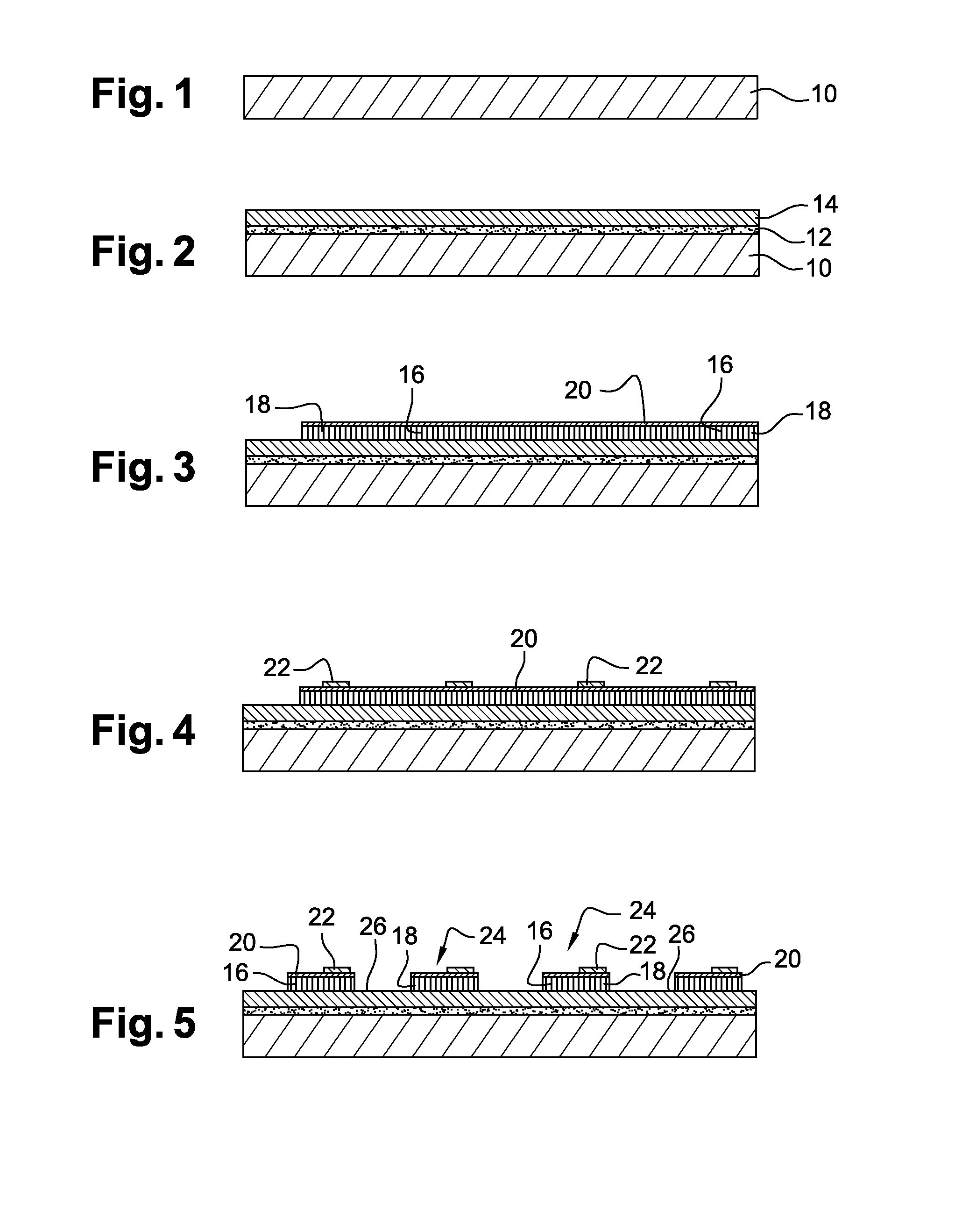
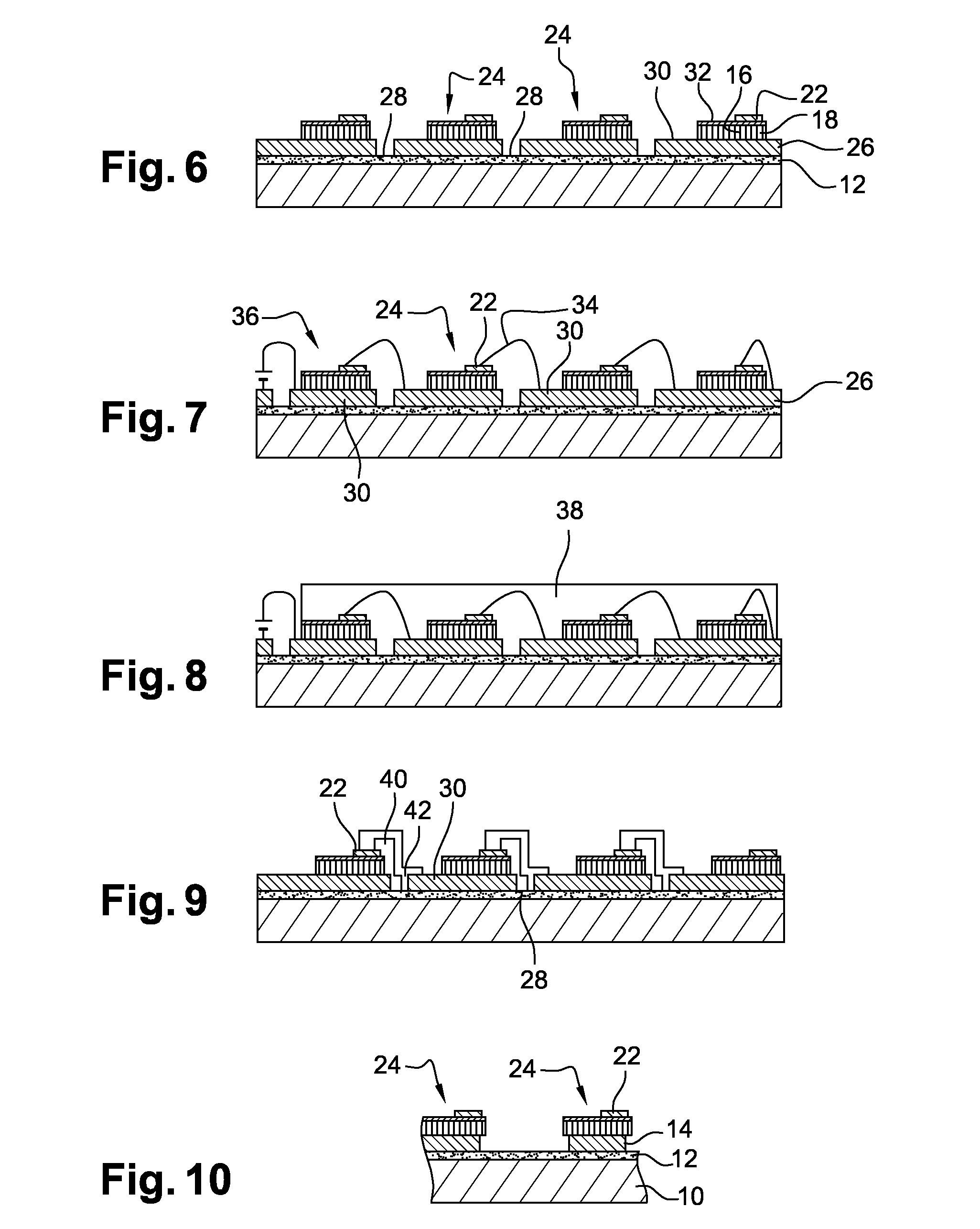
[0032]FIGS. 1 to 8 illustrate the main steps of a method of manufacturing an LED-based light emission device in accordance with the invention.

[0033]As illustrated in FIG. 1, the method begins with the formation of a monolithic or multilayer substrate 10. Apart from the function of support for elements constituting the LED-based light emission device, the substrate 10 is chosen so as to present a high thermal conductivity in order to dissipate the heat produced by the LEDs that will subsequently be formed thereon. The substrate 10 preferentially takes the form of a radiator with fins, as will be explained in more detail hereinafter.

[0034]The material or materials which form the substrate 10 are preferably selected from good thermal conductors. For example, the substrate 10 may be composed of one or more metals, or metal alloys, such as copper (Cu), silver (Ag), tungsten (W), aluminium (Al), molybdenum (Mo), nickel (Ni), vanadium (V), palladium (Pd), platinum (Pt), titanium (Ti) and i...


PUM


Abstract

A method of manufacturing a device based on LEDs includes the growth of semiconducting nanowires on a first electrode produced on an insulating face, and encapsulation thereof in planarising material; the formation, on the planarising material, of a second electrode with contact take-up areas. LEDs are formed by releasing a band of the first electrode around each take-up area, including forming a mask defining the bands on the second electrode, chemically etching the planarising material, stopped so as to preserve planarising material, chemically etching the portion of nanowires thus released, and then chemically etching the remaining planarising material. A trench is formed along each of the bands as far as the insulating face and the LEDs are placed in series by connecting the take-up areas and bands of the first electrode.

Description

CROSS-REFERENCE TO RELATED APPLICATIONS[0001]The present application is a National Stage Application of PCT International Application No. PCT / FR2010 / 051553 (filed on Jul. 22, 2010), under 35 U.S.C. §371, which claims priority to French Patent Application No. 0955697 (tiled on Aug. 18, 2009), which are each hereby incorporated by reference in their respective entireties.FIELD OF THE INVENTION[0002]The present invention relates to the field of the manufacture of light emission devices based on light emitting diodes, in particular, emission devices of high brightness and with a large surface area.BACKGROUND OF THE INVENTION[0003]Usually a light emission device based on LEDs (the acronym for light emitting diodes) consists of a stack of semiconductor layers produced by epitaxy on a sapphire or silicon carbide (SiC) substrate having a mesh parameter suited to the material of the semiconductor layers. A plurality of diodes is usually simultaneously produced to the scale of a wafer, and th...

Claims


Application Information

Patent Timeline
IPC IPC(8): H01L33/50
CPCH01L21/02425H01L21/02488H01L2924/0002H01L33/62H01L33/18H01L21/02491H01L21/02502H01L21/02521H01L21/0254H01L21/02554H01L21/02603H01L27/153H01L33/06H01L33/08H01L2224/48091H01L2924/00014H01L2924/00
Inventor GASSE, ADRIENGILET, PHILIPPE
Owner COMMISSARIAT A LENERGIE ATOMIQUE ET AUX ENERGIES ALTERNATIVES
Why Eureka
Try Eureka