

Micromechanical component and manufacturing method for a micromechanical component
- Summary
- Abstract
- Description
- Claims
- Application Information
AI Technical Summary
Benefits of technology
Problems solved by technology
Method used
Image

Examples
Embodiment Construction
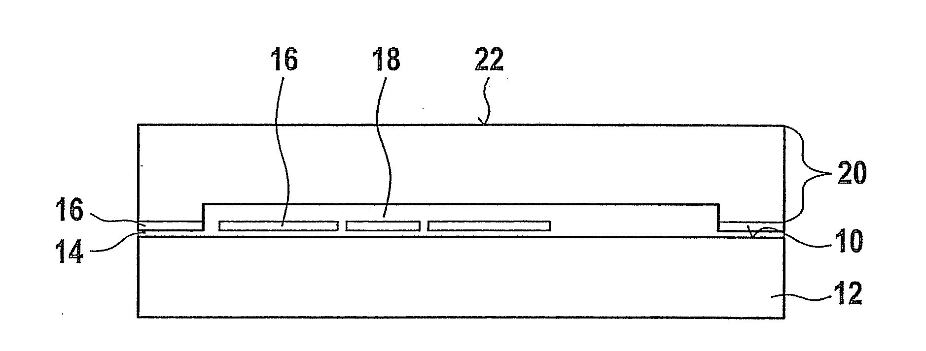
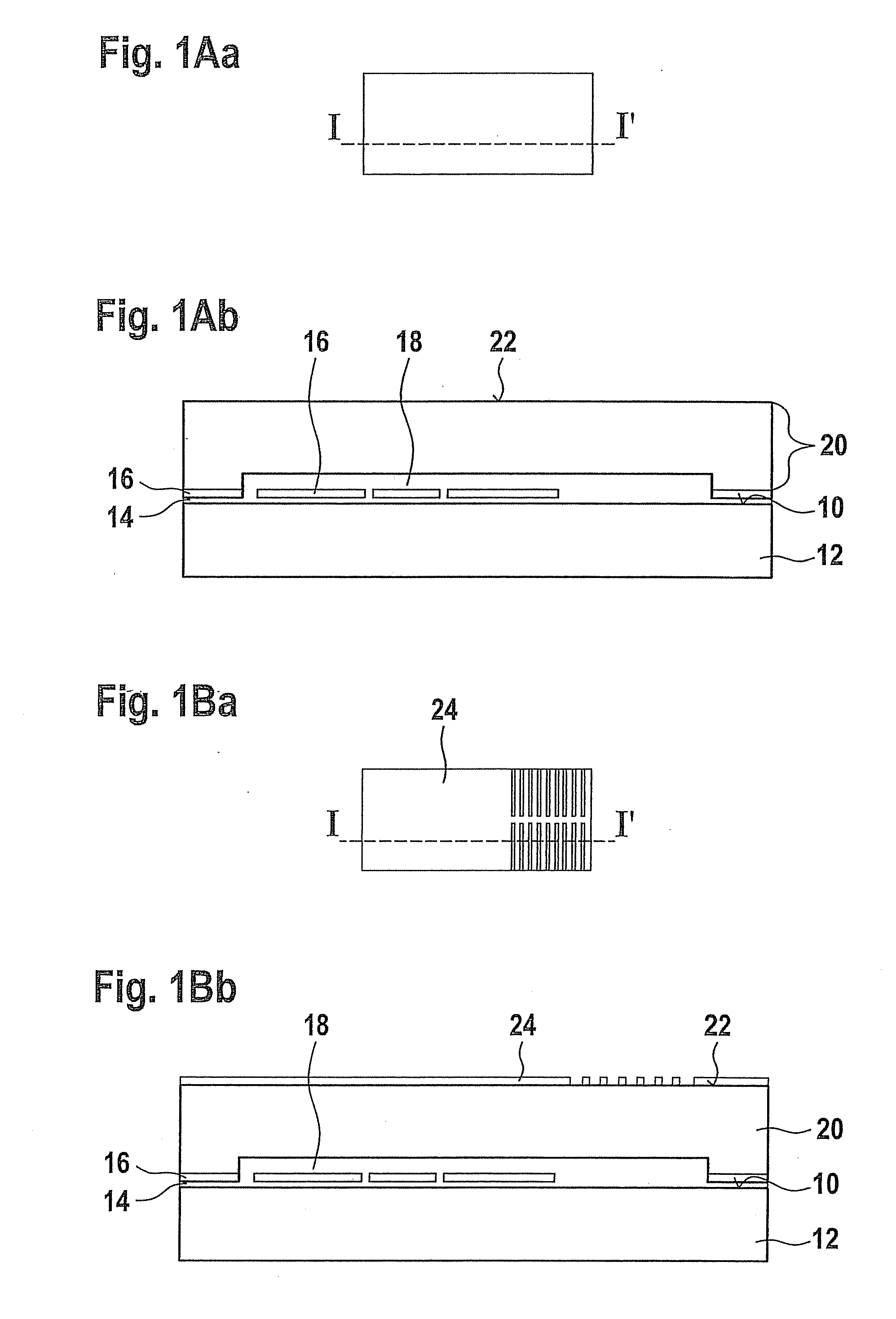
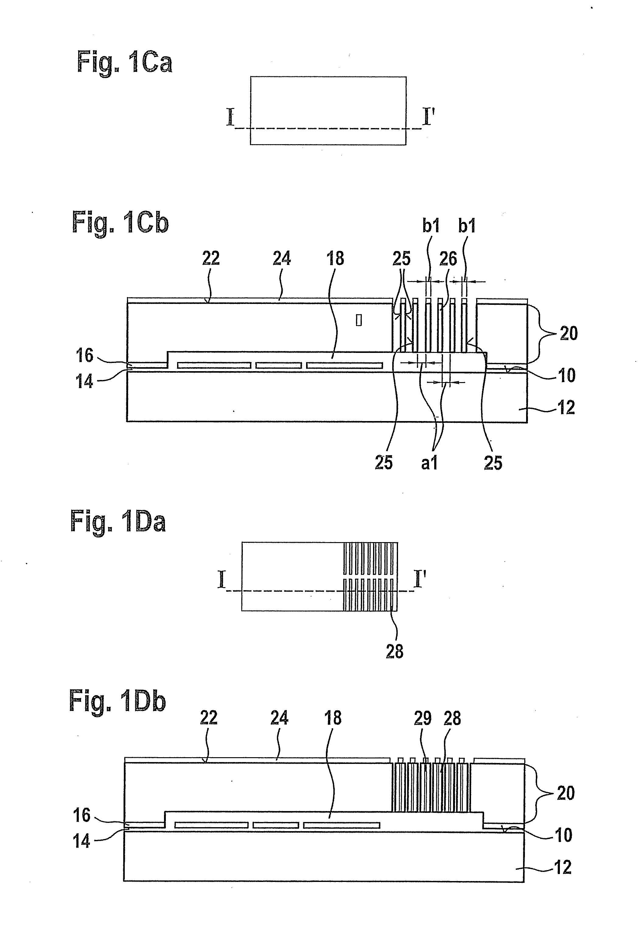
[0024]In the following, the technology according to the present invention is described with reference to micromechanical components and manufacturing methods for micromechanical components, the micromechanical components being designed as acceleration sensors for detecting and / or establishing (measuring) an acceleration and / or an acceleration component in a spatial direction perpendicular to the surface of the seismic weight of the micromechanical component, present in its (zero-acceleration) starting position. However, it is pointed out that the technology according to the present invention is not limited to such micromechanical components and methods for their manufacture.
[0025]For example, using the technology according to the present invention, an acceleration sensor may also be manufactured / provided, by which an acceleration in two spatial directions (preferably oriented perpendicularly to one another), or two acceleration components, are detectable and / or determinable (measura...
PUM
| Property | Measurement | Unit |
|---|---|---|
| Time | aaaaa | aaaaa |
| Weight | aaaaa | aaaaa |
| Density | aaaaa | aaaaa |
Abstract
Description
Claims
Application Information