Microchannel plate and its manufacturing method

a microchannel plate and manufacturing method technology, applied in the field of microchannel plates, can solve the problems of low resistivity of bulk crystalline materials, complex process, and high cost, and achieve the effect of maintaining a large open area ratio, and reducing the cost of production

Active Publication Date: 2012-07-26
ECOLE POLYTECHNIQUE FEDERALE DE LAUSANNE (EPFL)
View PDF1 Cites 0 Cited by
  • Summary
  • Abstract
  • Description
  • Claims
  • Application Information

AI Technical Summary

Problems solved by technology

The process is complex and costly.
However, low resistivity of bulk crystalline requires an extra oxidation film and a deposition of a semiconducting layer.
By fusing, drawing, and etching it is impossible or prohibitively expensive to make channel diameters below 5 μm and maintain a large open area ratio.
The drawbacks of current MCP are that:a slow recharging time constant is associated with each microchannel after one secondary electron emission avalanche event, a dead time in the order of 10 ms, limiting gain and counting rate capability.besides material issues, existing MCP do not have an easy readout for finely pixilated imaging device.current MCP technologies do not provide the integration of the MCP device with the imaging readout system.current etching methods limit miniaturization of pore diameters to 5 μm.

Method used


Image

  • Microchannel plate and its manufacturing method
  • Microchannel plate and its manufacturing method
  • Microchannel plate and its manufacturing method

Examples


example

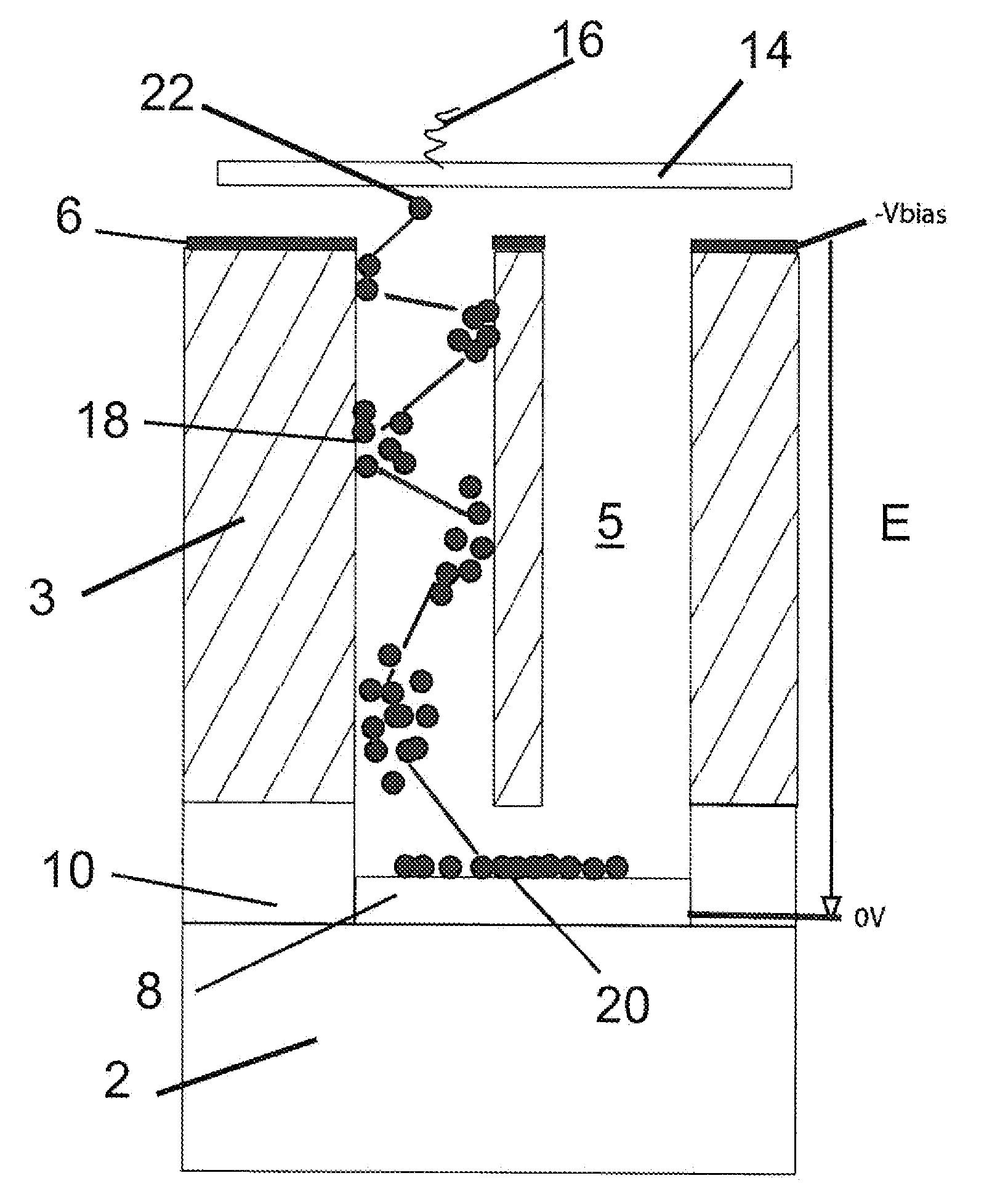
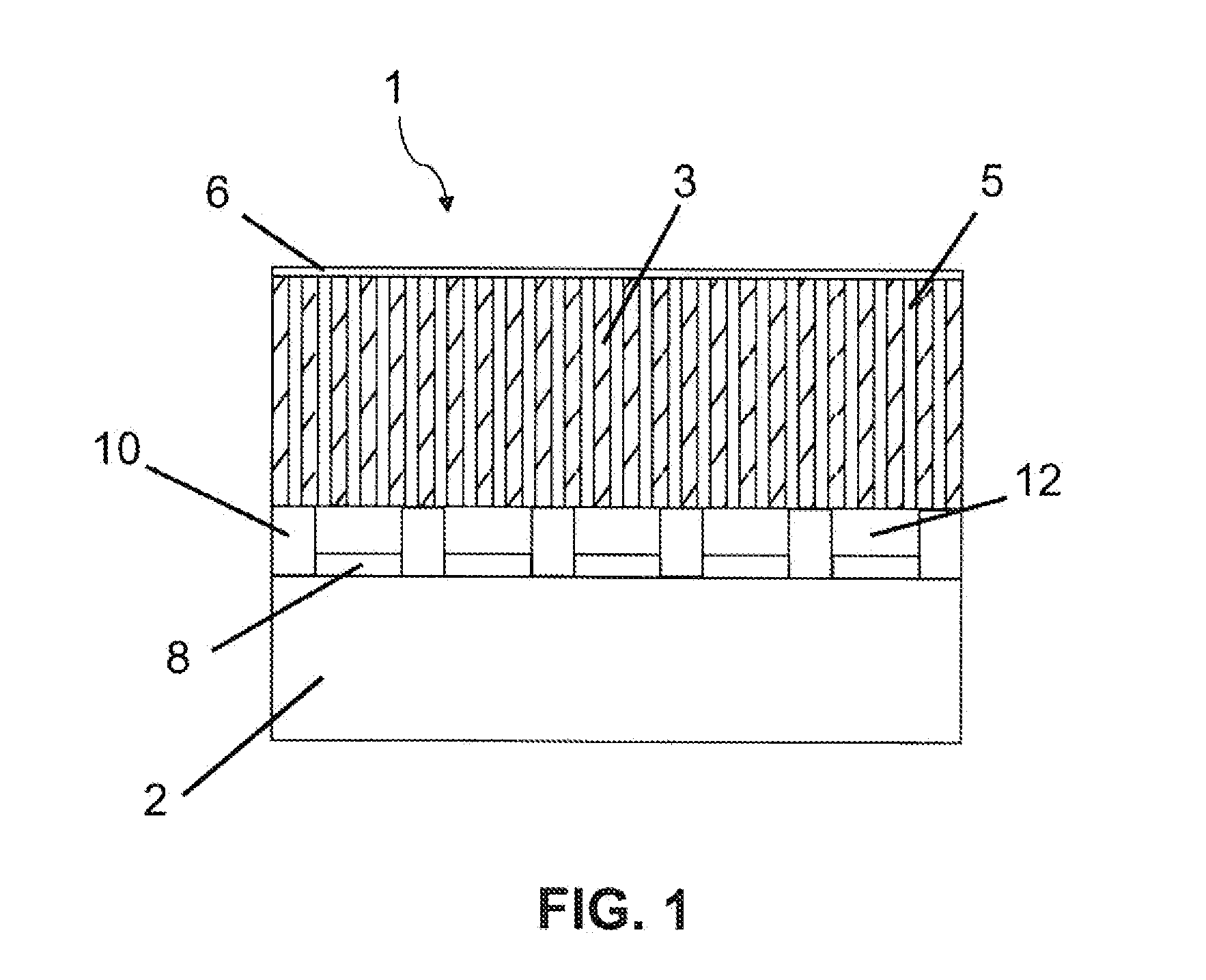
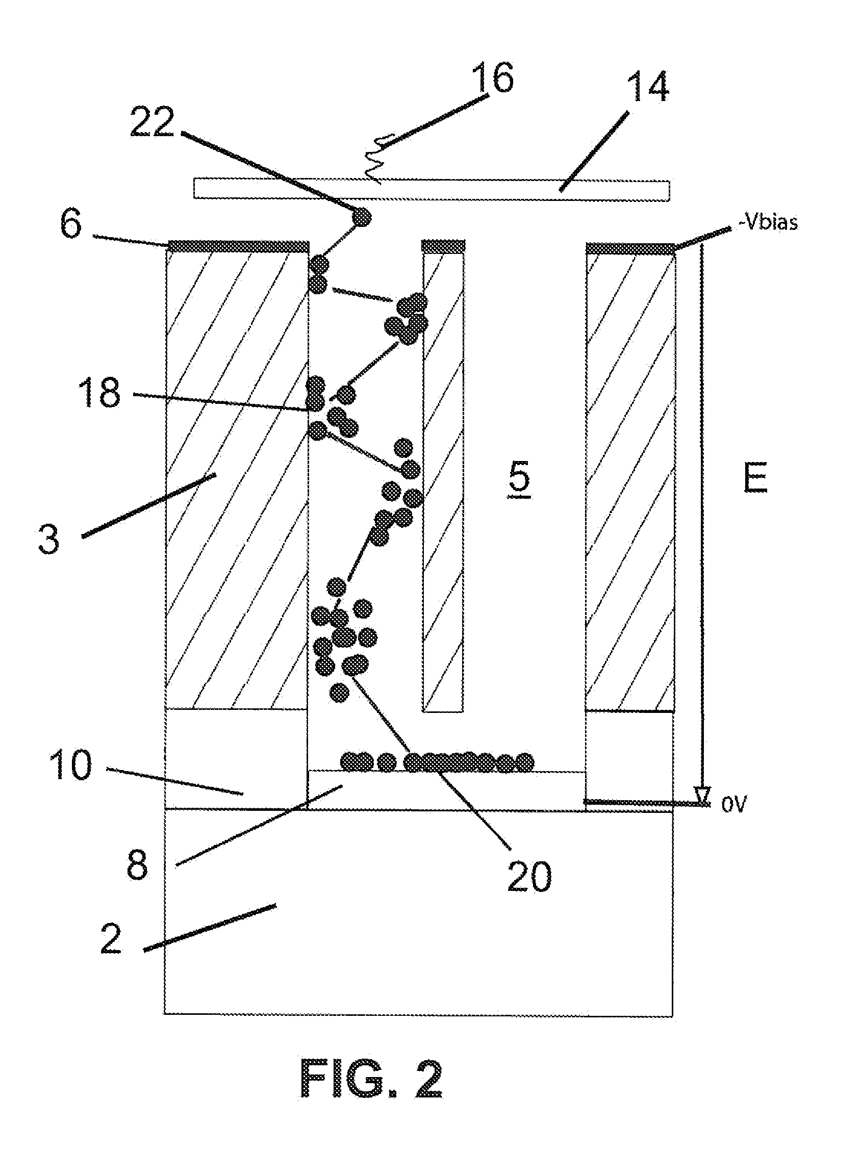
[0077]A microchannel plate of the invention was obtained by using, as passive substrate, an oxidized silicon wafer with pixel collecting electrodes. An intrinsic hydrogenated amorphous silicon film was deposited on said substrate by PECVD, with a thickness of 100 μm. An array of microchannels was formed by DRIE, the channels having a diameter of 3 μm.

[0078]The current was measured on a microchannel plate pixel as a function of the microchannel plate bias voltage and beam intensity for an electron beam focused on the sample. The results are shown in FIG. 3. The curve A corresponds to no beam, the curve B corresponds to a beam of 1.06 A, the curve C corresponds to a beam of 1.31 A, and the curve D corresponds to a beam of 1.56 A. Increase in the bias voltage enhanced the response of the microchannel plate (amplification of the incoming electron beams).


PUM

PropertyMeasurementUnit
thicknessaaaaaaaaaa
thicknessaaaaaaaaaa
thicknessaaaaaaaaaa

Abstract

A microchannel plate (1) having an array of channels (5),includes a substrate (2) and, deposited on the substrate, a hydrogenated amorphous silicon film (3) having a thickness ranging between 50 μm and 200 μm, preferably between 80 μm and 120 μm, the film including the array of channels (5). Preferably, the substrate (2) is an integrated circuit having an internal electronic readout circuit and pixilated collection electrodes (8), and the film (3) is integrated on the substrate (2). The channels (5) may be formed by a Deep Reactive Ion Etching (DRIE) process.

Description

TECHNICAL FIELD[0001]The present invention relates to a microchannel plate (“MCP”), and its manufacturing method. The present invention relates also to an electron multiplier imaging device comprising such microchannel plate.BACKGROUND OF THE INVENTION[0002]MCP's have been firstly used in image intensifier tubes for night / low light vision applications to amplify ambient light into a useful image. A typical intensifier device is a vacuum device, with a photocathode and a microchannel plate (“MCP”), and a phosphor screen with adaptation optics. Incoming photons strike the photocathode and converts photons to electrons, which are accelerated toward the MCP by an electric field. The MCP has many microchannels, each of which functions as an independent electron amplifier. The amplified electron image of the MCP excites a phosphor screen or a CCD or any other imaging device.[0003]Detection and amplification of low-level image signals or single photon or particle detection is a critical fu...

Claims


Application Information

Patent Timeline
Patent Type & Authority Applications(United States)
IPC IPC(8): H01J43/06B05D3/10C23C16/24H01J43/04B05D5/12
CPCH01J43/246
Inventor JARRON, PIERREWYRSCH, NICOLAS
Owner ECOLE POLYTECHNIQUE FEDERALE DE LAUSANNE (EPFL)
Why Eureka
Try Eureka