Semiconductor device

a technology of semiconductor memory devices and integrated circuits, which is applied in the direction of transistors, solid-state devices, instruments, etc., can solve the problems of large power consumption, deterioration of transistors, and significant problems, and achieve the effect of improving data retention characteristics of semiconductor memory devices, high reliability, and reducing power consumption

Inactive Publication Date: 2012-07-26
SEMICON ENERGY LAB CO LTD
View PDF5 Cites 37 Cited by
  • Summary
  • Abstract
  • Description
  • Claims
  • Application Information

AI Technical Summary

Benefits of technology

[0015]The thickness of the oxide semiconductor layer is preferably greater than or equal to 1 nm and less than or equal to 100 nm, and the oxide semiconductor layer may be a crystalline oxide semiconductor layer. With the crystalline oxide semiconductor layer, it is possible to provide a highly reliable semiconductor device in which changes of the electrical characteristics of the transistor due to irradiation with visible light or ultraviolet light can be suppressed. Further, the crystalline oxide semiconductor layer includes an oxide including a crystal with c-axis alignment (also referred to as c-axis aligned crystal (CAAC)), which has neither a single crystal structure nor an amorphous structure.
[0016]A technique that can improve data retention characteristics of a semiconductor memory device can be provided.
[0017]A technique that can reduce power consumption as well as improving data retention characteristics of a semiconductor memory device can also be provided.
[0018]A technique that can decrease the area of a semiconductor device as well as improving data retention characteristics and reducing power consumption of the semiconductor device can also be provided.

Problems solved by technology

However, a conventional DRAM needs to be refreshed at an interval of several tens of milliseconds to hold data, which results in large power consumption.
In addition, a transistor therein is frequently turned on and off; thus, deterioration of the transistor is also a problem.
These problems become significant as the memory capacity increases and transistor miniaturization advances.
Another problem is an increase in the area of a semiconductor device.

Method used


Image

  • Semiconductor device
  • Semiconductor device
  • Semiconductor device

Examples


embodiment 1

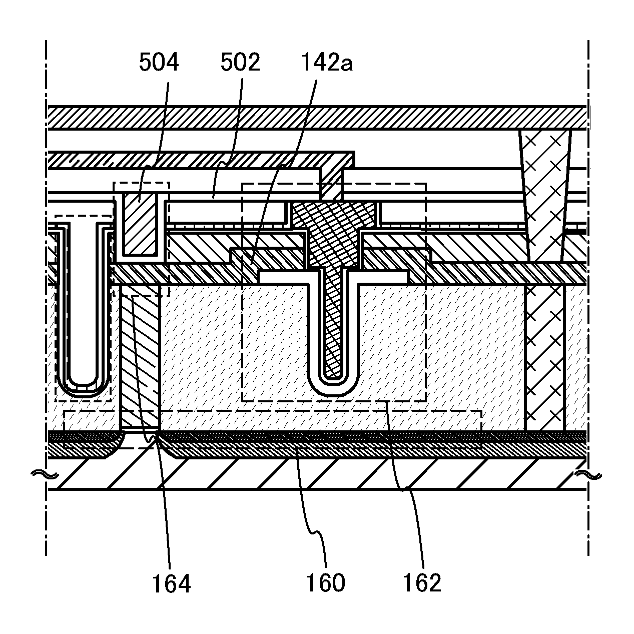
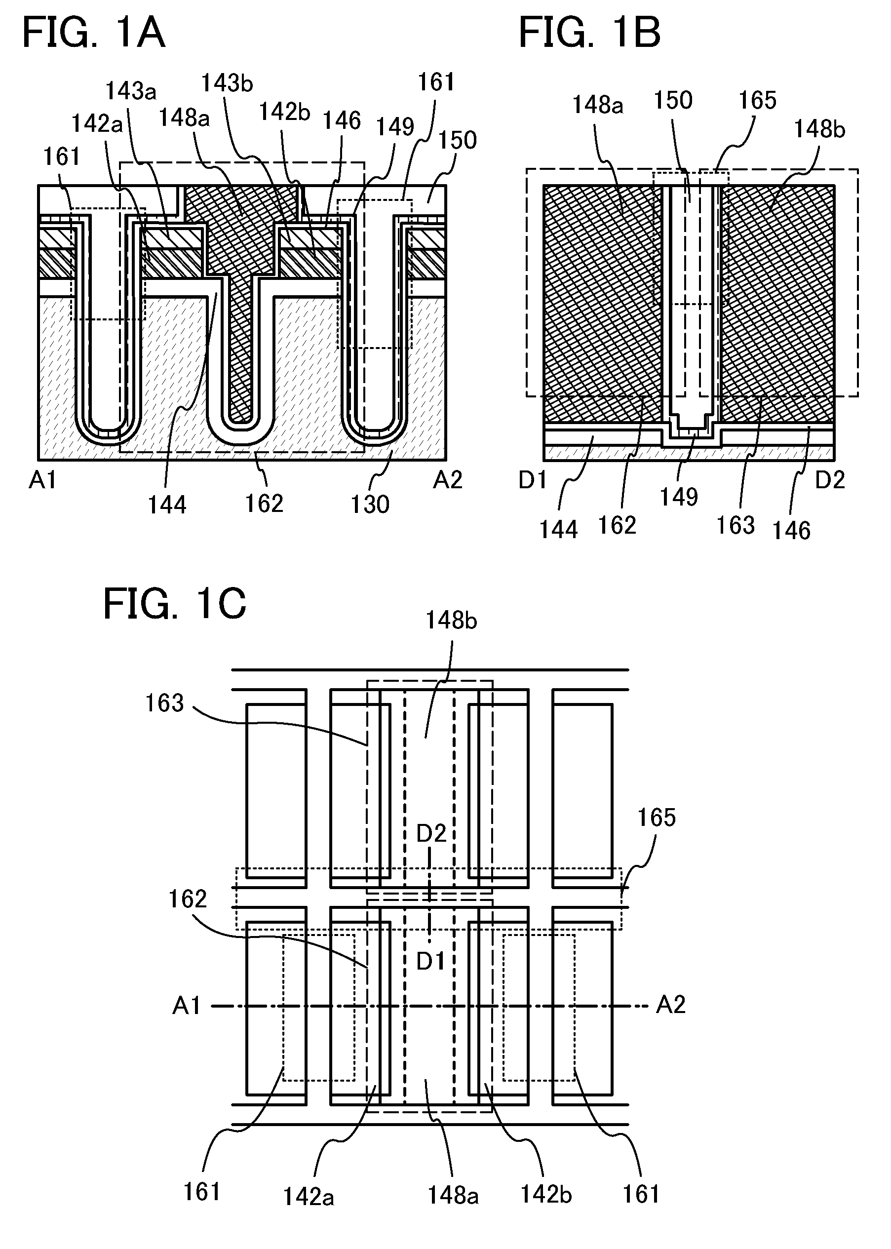
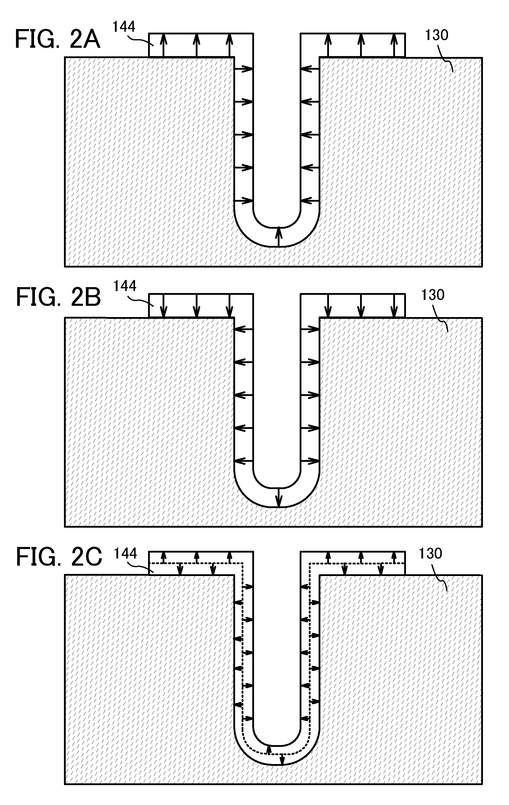
[0037]In this embodiment, a structure of a transistor and a method for manufacturing the transistor according to one embodiment of the present invention will be described with reference to FIGS. 1A to 1C and FIGS. 2A to 2C. FIG. 1A is an example of a cross-sectional view of a transistor 162 in a channel-length direction. FIG. 1B is an example of a cross-sectional view perpendicular to an element isolation region 165 between the transistor 162 and a transistor 163. FIG. 1C is an example of a top view of the transistor 162 and the transistor 163. Note that FIG. 1B is part of a cross-sectional view of the transistor 162 in a channel-width direction, and corresponds to a cross-sectional view taken along a dotted line D1-D2 in FIG. 1C. FIG. 1A corresponds to a cross-sectional view taken along a dotted line A1-A2 in FIG. 1C.

[0038]First, an insulating layer 130 is formed with an oxide film over a semiconductor substrate. Then, a plurality of trenches (also referred to as grooves) is formed...

embodiment 2

[0117]In this embodiment, a semiconductor device which includes the transistor 162 illustrated in FIGS. 1A to 1C, which can hold stored data even when not powered, which has an unlimited number of write cycles, and which has a structure different from the structure described in Embodiment 2 will be described with reference to FIG. 4.

[0118]The semiconductor device illustrated in FIG. 4 includes a transistor 350 including a first semiconductor material in a lower portion, and a transistor 162 including a second semiconductor material in an upper portion. Note that in this embodiment, the transistor 350 formed in the lower portion is referred to as a first transistor, and the transistor 162 formed in the upper portion is referred to as a second transistor. Although a plurality of transistors is formed in the upper and lower portions, the transistor 350 and the transistor 162 will be typically described. A plurality of transistors including the transistor 350 which is formed in the lowe...

embodiment 4

[0141]In this embodiment, a semiconductor device which includes the transistor 162 illustrated in FIGS. 1A to 1C, which can hold stored data even when not powered, which has an unlimited number of write cycles, and which has a structure different from the structures described in Embodiments 2 and 3 will be described with reference to FIGS. 5A and 5B and FIG. 6.

[0142]FIG. 5A illustrates an example of a circuit configuration of a semiconductor device, and FIG. 5B is a conceptual diagram illustrating an example of a semiconductor device. First, the semiconductor device illustrated in FIG. 5A will be described, and then, the semiconductor device illustrated in FIG. 5B will be described.

[0143]In the semiconductor device illustrated in FIG. 5A, a bit line BL is electrically connected to a source electrode or a drain electrode of the transistor 162, a word line WL is electrically connected to a gate electrode of the transistor 162, and a source electrode or a drain electrode of the transis...


PUM

PropertyMeasurementUnit
channel lengthaaaaaaaaaa
thicknessaaaaaaaaaa
depthaaaaaaaaaa

Abstract

A conventional DRAM needs to be refreshed at an interval of several tens of milliseconds to hold data, which results in large power consumption. In addition, a transistor therein is frequently turned on and off; thus, deterioration of the transistor is also a problem. These problems become significant as the memory capacity increases and transistor miniaturization advances. Another problem is that an increase in memory capacity leads to an increase in the area, despite an attempt at integration through advancement of transistor miniaturization. A transistor is provided which includes an oxide semiconductor and has a trench structure including a trench for a gate electrode and a trench for element isolation. In addition, a plurality of memory elements each including the transistor having a trench structure and including an oxide semiconductor is stacked in a semiconductor device, whereby the circuit area of the semiconductor device can be reduced.

Description

TECHNICAL FIELD[0001]The present invention relates to a technique for miniaturizing semiconductor integrated circuits. The invention disclosed in this specification includes in its scope an element formed using a compound semiconductor, in addition to that formed using a silicon semiconductor, as a component of a semiconductor integrated circuit, and discloses an element formed using an oxide semiconductor as an example.BACKGROUND ART[0002]As semiconductor memory devices, dynamic RAMs (DRAMs) are well-known products and currently used in a variety of electronic devices. A memory cell which is a key component in a DRAM includes a read and write transistor and a capacitor.[0003]Circuit patterns for DRAMs, like those for other semiconductor integrated circuits, have been miniaturized in accordance with the scaling law, and there was a time when it was considered difficult to achieve a design rule of 100 nm or less. One of the reasons is that in a transistor having a channel length of 1...

Claims


Application Information

Patent Timeline
Patent Type & Authority Applications(United States)
IPC IPC(8): H01L29/16H01L27/108
CPCH01L27/0688H01L27/10873H01L27/11526H01L27/11551H01L27/1156H01L29/7833H01L27/1225H01L28/60G11C11/403H01L29/78H01L27/1207H10B12/05H10B41/40H10B41/20H10B41/70
Inventor YAMAZAKI, SHUNPEIGODO, HIROMICHI
Owner SEMICON ENERGY LAB CO LTD
Why Eureka
Try Eureka